Liquid crystal display panel, electronic apparatus, and manufacturing method thereof

Active Publication Date: 2008-12-04
AU OPTRONICS CORP
View PDF8 Cites 27 Cited by
  • Summary
  • Abstract
  • Description
  • Claims
  • Application Information

AI Technical Summary

Benefits of technology

[0011]The present invention is further provided to an electronic ap

Problems solved by technology

One of the conventional issues lies in that light leakage arisen from the disclination of the liquid crystal molecules surrounding the alignment protrusions and the alignment slits leads to a reduction in a display contrast ratio of the LCD panel.
However, an aperture ratio of the display is limited or reduced thereby.
Unfor

Method used


Image

  • Liquid crystal display panel, electronic apparatus, and manufacturing method thereof
  • Liquid crystal display panel, electronic apparatus, and manufacturing method thereof
  • Liquid crystal display panel, electronic apparatus, and manufacturing method thereof

Examples


Embodiment Construction

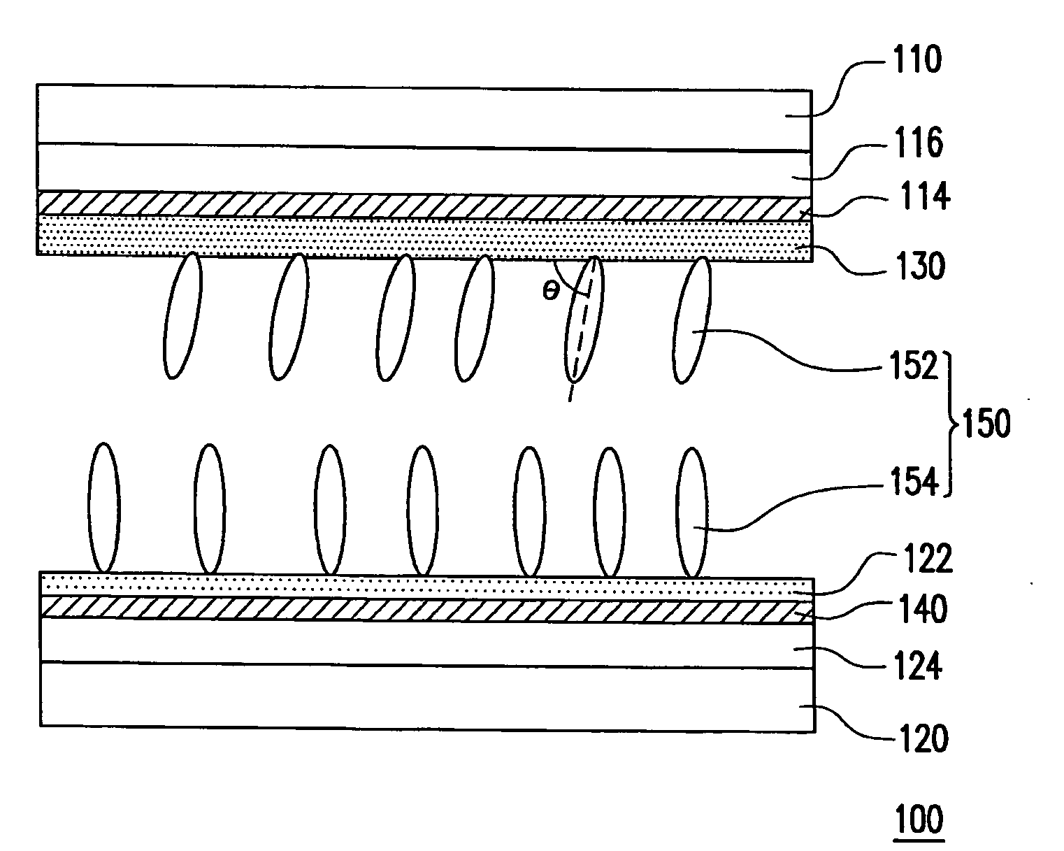
[0023]FIG. 1 is a schematic cross-sectional view of a liquid crystal display (LCD) panel according to an embodiment of the present invention. Referring to FIG. 1, an LCD panel 100 includes a first substrate 110, a second substrate 120, a photo-alignment layer 130, a plurality of patterned pixel electrodes 140, and a liquid crystal layer 150. The second substrate 120 is opposite to the first substrate 110. The photo-alignment layer 130 is disposed on a surface of the first substrate 110, and the surface of the first substrate 110 faces the second substrate 120. The patterned pixel electrodes 140 are disposed on a surface of the second substrate 120, and the surface of the second substrate 120 faces the first substrate 110. The liquid crystal layer 150 is disposed between the first substrate 110 and the second substrate 120. In addition, the patterned pixel electrodes 140 are, for example, arranged in array on the second substrate 120, but the arrangement of the patterned pixel electr...


PUM


Abstract

A method for manufacturing a liquid crystal display panel is provided. A photo-alignment layer is formed on a first substrate. Patterned pixel electrodes including intersected electrodes and stripe electrodes are formed on a second substrate. A liquid crystal layer is formed between the photo-alignment layer and the patterned pixel electrodes. Each intersected electrode has a first directional portion and a second directional portion interlacing thereto. The stripe electrodes with silts connect the first and/or the second directional portions. When an electric field between the first and the second substrates is substantially zero, liquid crystal molecules near the photo-alignment layer are arranged at a pre-tilt angle, while those disposed at another side near the second substrate are substantially perpendicular to the second substrate. As the liquid crystal layer is driven, the liquid crystal molecules of the liquid crystal layer are substantially arranged along an extending direction of the slits.

Description

CROSS-REFERENCE TO RELATED APPLICATION[0001]This application claims the priority benefit of Taiwan application serial no. 96119753, filed Jun. 1, 2007. All disclosure of the Taiwan application is incorporated herein by reference.BACKGROUND OF THE INVENTION[0002]1. Field of the Invention[0003]The present invention relates to a liquid crystal display (LCD) panel, an electronic apparatus, a method for manufacturing the LCD panel, and a method for manufacturing the electronic apparatus and, more particularly, relates to an LCD and an electronic apparatus having a photo-alignment film and patterned pixel electrodes with micro slits disposed therein, and methods for manufacturing the LCD panel and the electronic apparatus.[0004]2. Description of Related Art[0005]Liquid crystal displays (LCDs) characterized by high contrast ratio, no gray scale inversion, little color shift, high luminance, full color, high color saturation, high responsive speed, and wide viewing angles are required in th...

Claims


Application Information

Patent Timeline
IPC IPC(8): G02F1/141H01L21/02
CPCG02F1/133707G02F1/133788G02F1/1393G02F2001/133757G02F2001/136236G02F2001/13787G02F1/133757G02F1/136236G02F1/13787
Inventor YANG, RONG-CHINGWU, MING-HUNGCHEN, CHIA-MINGKUO, YU-PING
Owner AU OPTRONICS CORP
Why Eureka
Try Eureka