Receiver and electronic device

a technology of electronic devices and receivers, applied in the field of receivers, can solve problems such as the inability to detect a defect in a pulse, the deterioration of the quality of the reproduced sound, and the reduction of the number of components, so as to reduce the discomfort of hearing

Inactive Publication Date: 2008-12-04
SHARP KK
View PDF5 Cites 2 Cited by
  • Summary
  • Abstract
  • Description
  • Claims
  • Application Information

AI Technical Summary

Benefits of technology

[0026]The present invention was done to solve the problem above, and an objective of the present invention is to provide a receiver which can reduce discomfort in hea

Problems solved by technology

In addition, in consideration of the downsizing of devices such as mobile phone terminals, the reduction in the number of components and the downsizing have become technical problems in the field of communications devices.
For example, in case where a variation in pulse width occurs in audio data to be received by a receiving infrared communication device, the DC (Direct Current) level of the audio data is unnecessarily varied and hence noise is superposed into the audio data, with the result that the quality of reproduced sound is deteriorated.
However, the technology disclosed by Patent Document 2 is unable to detect a defect in a pulse, which is a result of conversion of the time density of a pulse into a voltage by a smoothing circuit and is small but is large enough to allow the voltage to be not lower than a predetermined threshold.
Furthermore, in the technology disclosed by Patent Document 2, it is not possible to detect a variation (e.g. pulse widening) of pulse width in the width direction of the pulse, with which a voltage value after the conversion by the smoothing circuit does not decrease.
However, with the technology disclosed in Patent Document 3, it is not possible to detect a defect in pulse, which is small but large enough to allow the number of times the output signal of the low-pass filter exceeds the predetermined threshold not to be below the transmission rate figured out by adding up the average transmission rates of the respective digital signals of plural channels.
Also, being similar to the technology disclosed by Patent Document 2, the technology disclosed by Patent Document 3 cannot detect a variation in pulse width in the width d

Method used


Image

  • Receiver and electronic device
  • Receiver and electronic device
  • Receiver and electronic device

Examples


embodiment 1

[0080]The following will discuss an embodiment of the present invention with reference to FIG. 1 through FIG. 6.

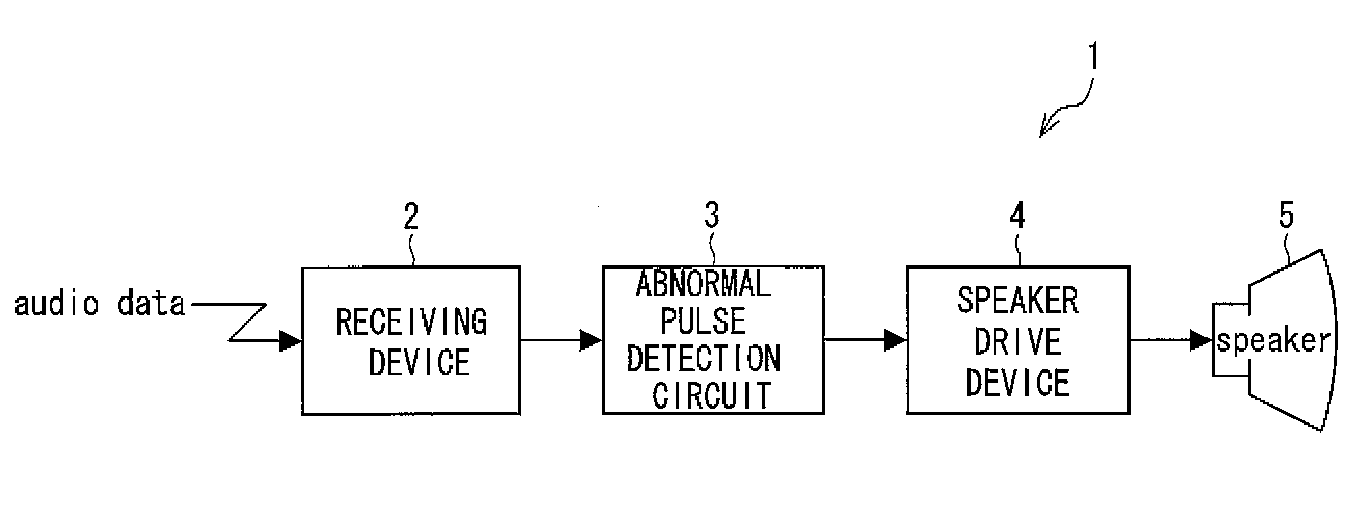
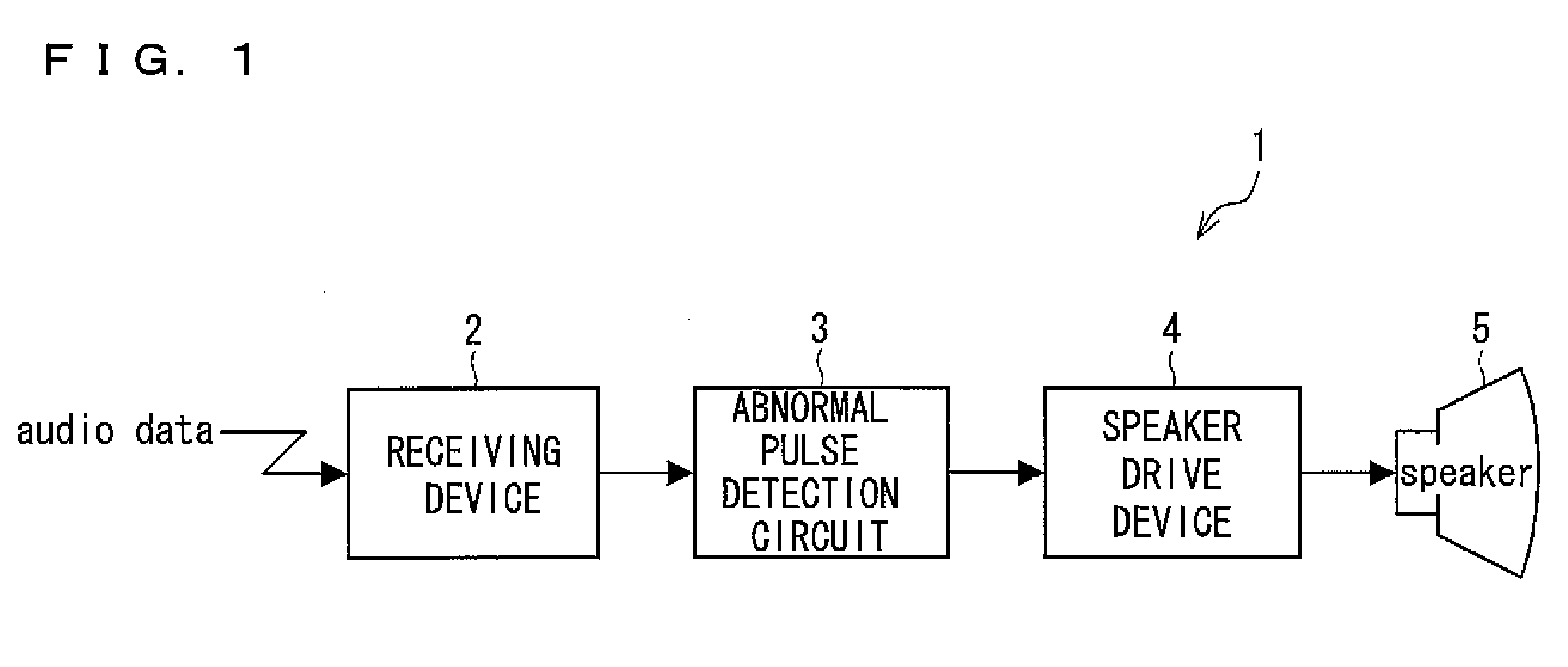
[0081]FIG. 1 is a block diagram showing the outline of a receiver of the present invention.

[0082]An optical receiver (receiver) 1 shown in FIG. 1 is, for example, a receiver provided in an electronic device which receives in a wireless manner an optical signal transmitted by a transmission system adopting infrared light or light, and includes a receiving device 2, an abnormal pulse detection circuit (abnormal pulse detection means) 3, a speaker driver 4, and a speaker 5.

[0083]The receiving device 2 receives in a wireless manner audio data supplied from, for example, an optical transmitter (not illustrated), and amplifies the received audio data. Then the receiving device 2 sends the amplified audio data to the abnormal pulse detection circuit 3. It is noted that in the present invention the receiving device 2 does not have to have the function of amplifying audio data. It ...

embodiment 2

[0183]The following will describe another embodiment of the present invention with reference to FIGS. 7 through 11. By the way, members having the same functions as those already described with reference to figures are given the same numbers, so that the descriptions are omitted for the sake of convenience.

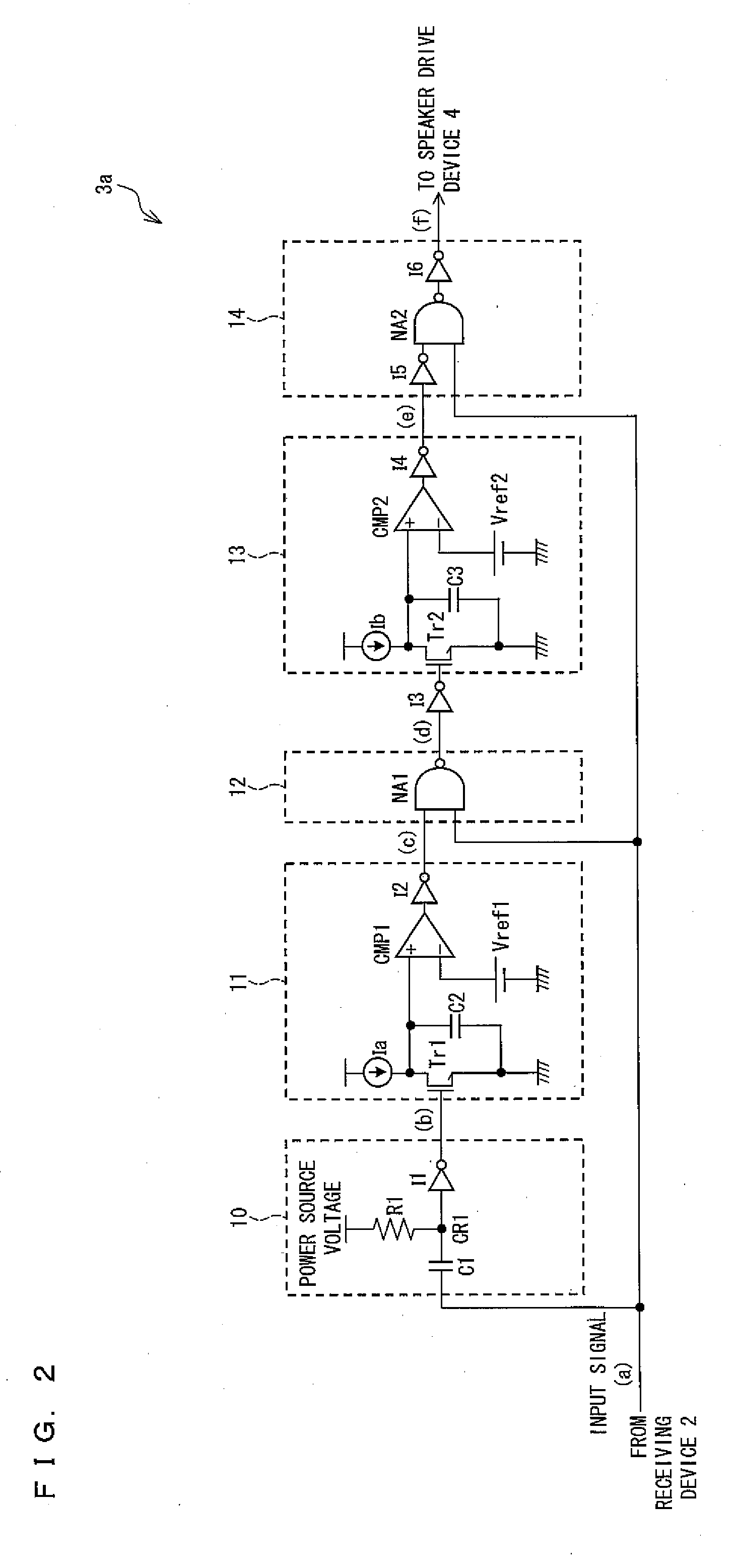
[0184]FIG. 7 is a block diagram showing another example of the abnormal pulse detection circuit. Being similar to the abnormal pulse detection circuit 3a shown in FIG. 2, the abnormal pulse detection circuit (abnormal pulse detection means) 3b shown in FIG. 7 is suitably used as an abnormal pulse detection circuit 3 in the optical receiver 1 shown in FIG. 1. The abnormal pulse detection circuit 3b shown in FIG. 7 receives a positive-logic digital signal as an input signal.

[0185]Being similar to the abnormal pulse detection circuit 3a shown in FIG. 2, the abnormal pulse detection circuit 3b shown in FIG. 7 is an example suitable for the detection of an abnormal pulse which occurs i...

embodiment 3

[0252]The following will describe another embodiment of the present invention with reference to FIGS. 12 through 14. By the way, members having the same functions as those already described with reference to figures are given the same numbers, so that the descriptions are omitted for the sake of convenience.

[0253]FIG. 12 is a block diagram showing a further example of the abnormal pulse detection circuit. Being similar to the abnormal pulse detection circuit 3a shown in FIG. 2 and the abnormal pulse detection circuit 3b shown in FIG. 7, the abnormal pulse detection circuit (abnormal pulse detection means) 3c shown in FIG. 12 is suitably used as the abnormal pulse detection circuit 3 in the optical receiver 1 shown in FIG. 1. The abnormal pulse detection circuit 3c shown in FIG. 12 receives a negative-logic digital signal as an input signal.

[0254]The abnormal pulse detection circuit 3c shown in FIG. 12 is an example suitable for detecting in the input signal an abnormal pulse (e.g. p...


PUM


Abstract

An abnormal pulse detection circuit in a receiver of the present invention includes: an incoming pulse edge detection circuit which detects the moment of rise of an input signal and outputs the result of the detection as an edge detection signal; a muting reference pulse generation circuit which generates a muting reference pulse based on the edge detection signal; a logic circuit which outputs a signal indicating a negative AND of the muting reference pulse and the input signal; a muting signal generation circuit which generates a muting signal from the output signal of the logic circuit; and a switching circuit which outputs the input signal or the muting signal. The receiver of the present invention can therefore reduce discomfort in hearing reproduced sound in case where a noise occurs in an audio signal due to a variation in pulse width.

Description

[0001]This Nonprovisional application claims priority under 35 U.S.C. § 119(a) on Patent Application No. 142638 / 2007 filed in Japan on May 29, 2007, Patent Application No. 290865 / 2007 filed in Japan on Nov. 8, 2007, and Patent Application No. 132223 / 2008 filed in Japan on May 20, 2008, the entire contents of which are hereby incorporated by reference.FIELD OF THE INVENTION[0002]The present invention relates to a receiver. The present invention particularly relates to a receiver which is provided in an electronic device or the like receiving a transmitted optical signal in a wireless manner, and which receives the optical signal as a data string constituted by a pulse train with a known pulse width.BACKGROUND OF THE INVENTION[0003]In the last the years, much effort has been made to develop an electronic device which processes an audio signal having been converted into digital data such as a one-bit data string. Such a device is advantageous in various ways for data communications bet...

Claims


Application Information

Patent Timeline
IPC IPC(8): H04B10/06
CPCH03F3/087H03K5/1252H04B10/1149H04B10/695
Inventor KAWABE, ISAMUYOKOGAWA, NARUICHI
Owner SHARP KK
Why Eureka
Try Eureka