Method and apparatus for debonding of structures which are bonded together, including (but not limited to) debonding of semiconductor wafers from carriers when the bonding is effected by double-sided adhesive tape

a technology of adhesive bonding and structure, applied in the direction of chemistry apparatus and processes, layered products, other domestic articles, etc., can solve the problems of non-uniform weakening of adhesive bond, complicated lifting off process, damage to wafer or carrier, etc., and achieve the effect of facilitating further separation of wafer and carrier

Inactive Publication Date: 2008-12-11
TRU SI TECH
View PDF2 Cites 55 Cited by
  • Summary
  • Abstract
  • Description
  • Claims
  • Application Information

AI Technical Summary

Benefits of technology

[0007]In addition, the inventors have observed that the gas emission from the tape may be non-uniform across the tape 130, resulting in non-uniform weakening of the adhesive bond. The lift-off should preferably start at a location at which the bond is weaker. In some embodiments, the lift-off is simultaneously attempt...

Problems solved by technology

If the lift-off is attempted too early, when the bond is still strong, the lift-off may be unsuccessful and may damage the wafer or the carrier.
Careful timing of the lift-off process is complicated because the appropriate lift-off time depends on the materials present in the wafer (as the...

Method used


Image

  • Method and apparatus for debonding of structures which are bonded together, including (but not limited to) debonding of semiconductor wafers from carriers when the bonding is effected by double-sided adhesive tape
  • Method and apparatus for debonding of structures which are bonded together, including (but not limited to) debonding of semiconductor wafers from carriers when the bonding is effected by double-sided adhesive tape
  • Method and apparatus for debonding of structures which are bonded together, including (but not limited to) debonding of semiconductor wafers from carriers when the bonding is effected by double-sided adhesive tape

Examples


Embodiment Construction

[0014]The embodiments described in this section illustrate but do not limit the invention. The invention is defined by the appended claims.

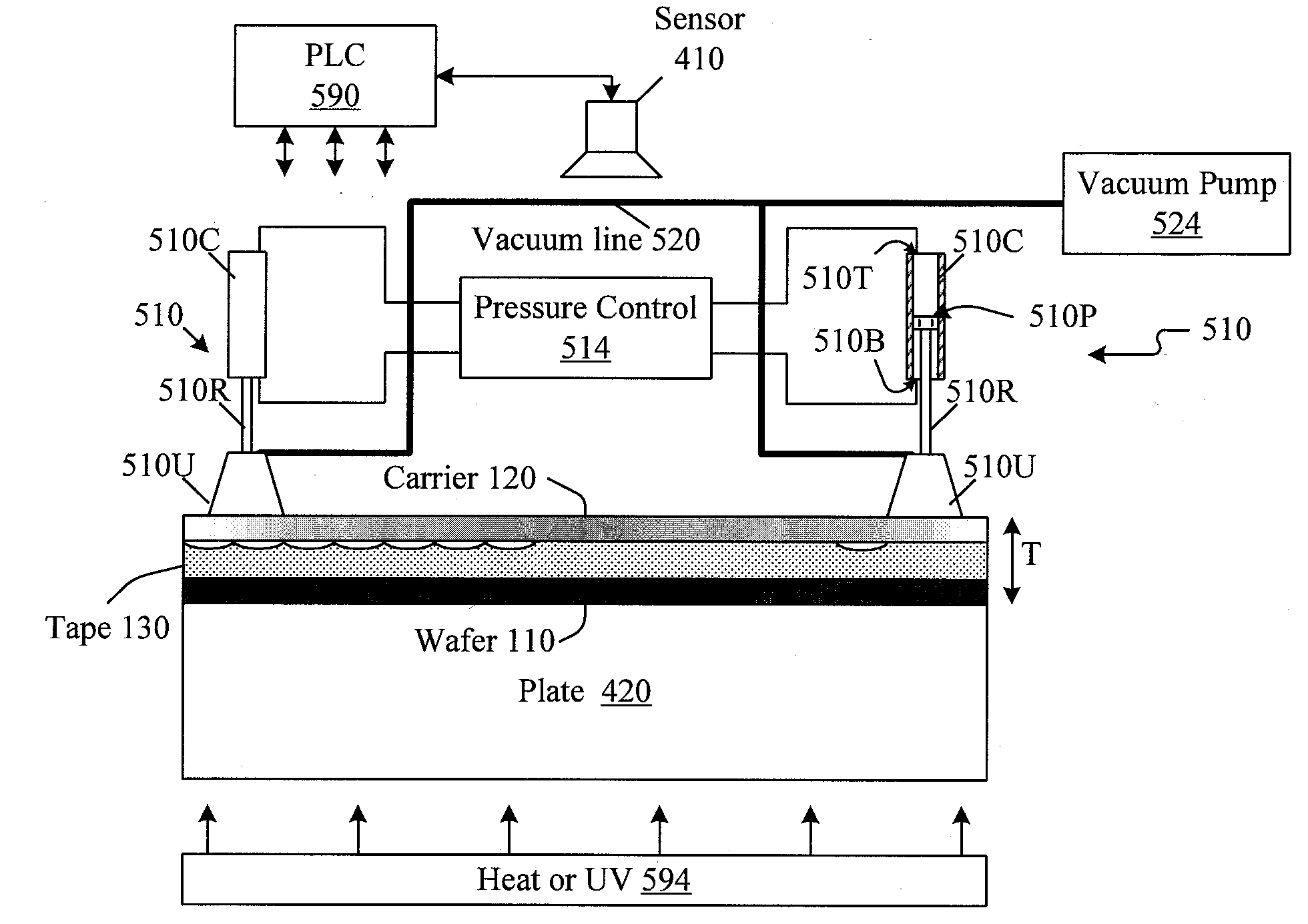
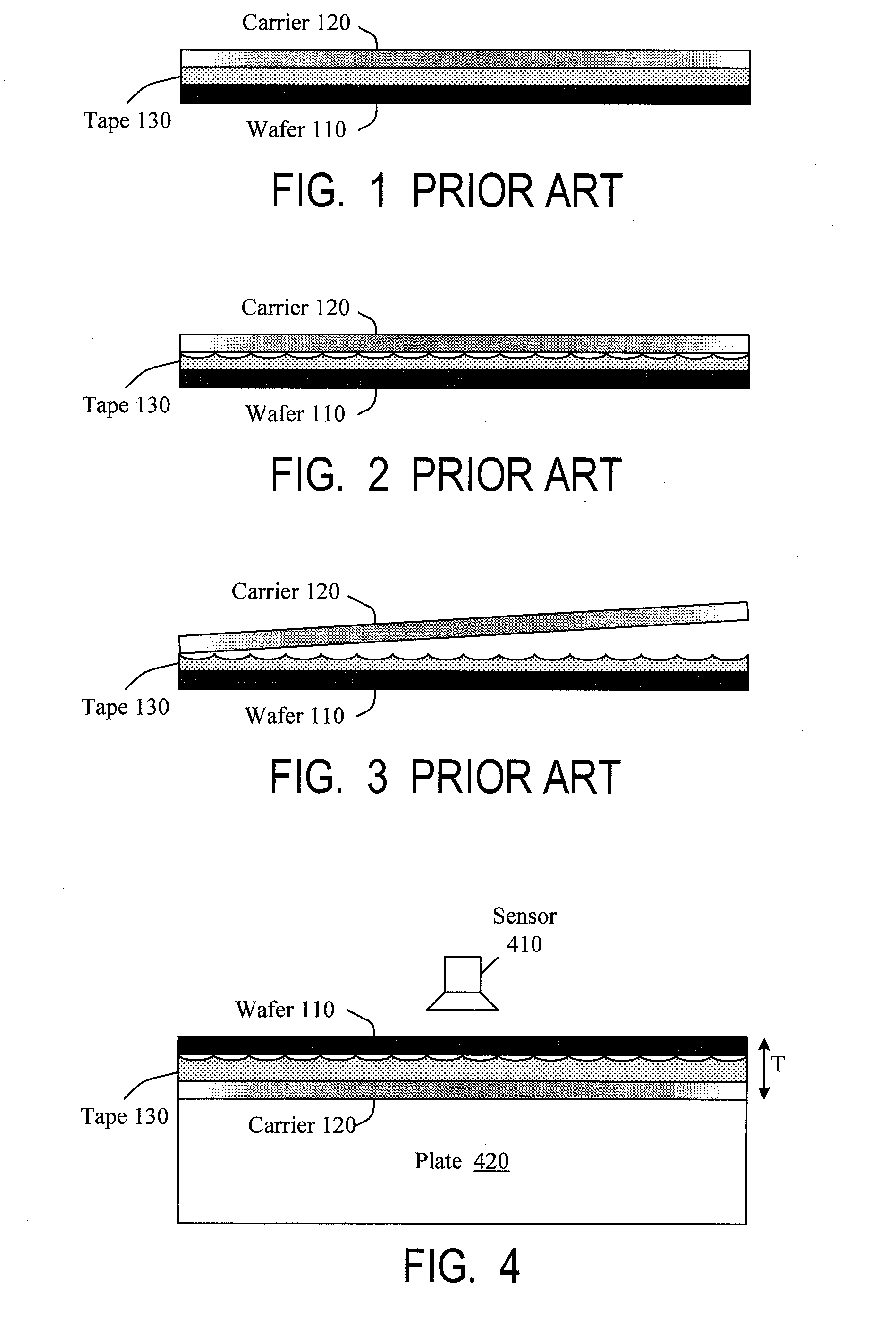
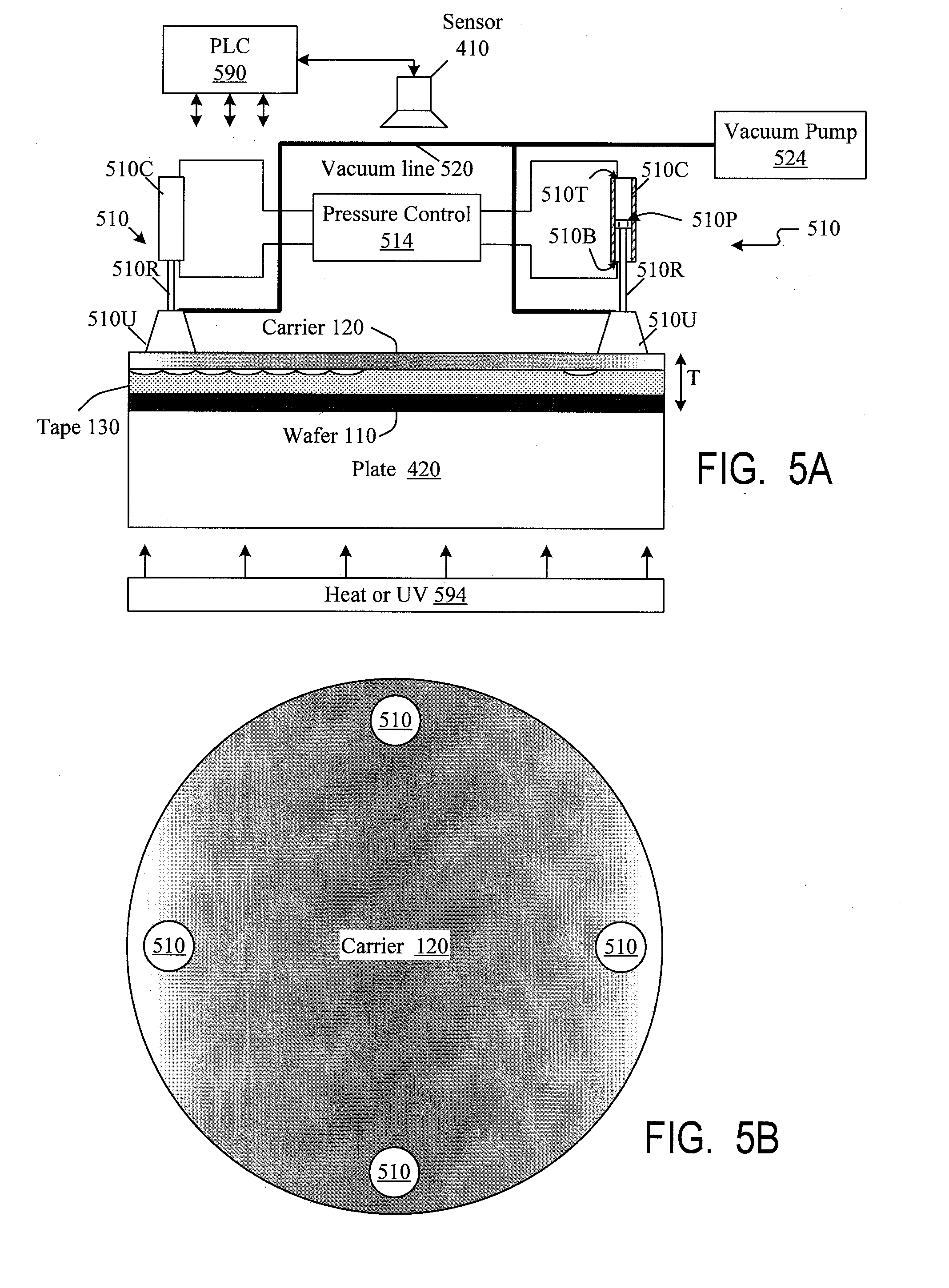
[0015]FIG. 4 illustrates a sensor 410 monitoring the thickness T of the structure consisting of semiconductor wafer 110 (e.g. a silicon wafer), carrier 120 (e.g. glass or silicon), and double-sided adhesive tape 130 bonding the wafer to the carrier. In FIG. 4, the gas emission from tape 130 occurs on the carrier side, but in other embodiments the gas emission may occur on the wafer side or on both sides. Wafer 110 can be a thick wafer, or can be a thin wafer tending to warp if left loose. The wafer rests on a plate 420, or is supported by a suitable chuck (e.g. a vacuum or electrostatic chuck, not shown), possibly by an end effector. The sensor can be a laser displacement sensor merely indicating the displacement of the top surface of carrier 120, or some other type of sensor. When the sensor's data indicate that the thickness T increases to a pr...


PUM

PropertyMeasurementUnit
Thicknessaaaaaaaaaa
Forceaaaaaaaaaa
Poweraaaaaaaaaa

Abstract

When heat or UV radiation is applied to an adhesive tape (130) which bonds a semiconductor wafer (110) to a carrier (120), the appropriate lift-off time for separating the wafer from the carrier is determined by monitoring the thickness (T or ΔT) of the wafer/tape/carrier sandwich. When the thickness or the thickness change has reached a predefined value or range of values, independently moveable driving members (510R) drive the wafer or the carrier with small forces at a plurality of spaced-apart locations along the periphery. As a result, the lift-off is initiated at the location of the weakest adhesion.

Description

BACKGROUND OF THE INVENTION[0001]The present invention relates to debonding of adhesively-bonded structures. Some embodiments involve debonding semiconductor wafers from carriers in fabrication of semiconductor integrated circuits.[0002]When a semiconductor wafer 110 (FIG. 1) is subjected to etching, depositions, photolithography, grinding, and other processes, the wafer can be bonded to a carrier 120 to strengthen the wafer against mechanical stresses and flatten the wafer if the wafer is warped. This is particularly desirable for thin, fragile wafers. A wafer can be initially thick but then thinned down while bonded to the carrier. The bonding can be performed with a double-sided adhesive tape 130. When the wafer has been processed as desired, the carrier must be debonded. Heat or UV radiation can be applied, depending on the type of tape 130, to cause gas emission from the adhesive on at least one side of tape 130 (top side in FIG. 2). The gas weakens the adhesive bond, and the c...

Claims


Application Information

Patent Timeline
IPC IPC(8): B32B38/10
CPCB32B37/06Y10T156/1158B32B2309/72B32B2310/0806B32B2310/0831B32B2457/14C09J5/00C09J5/06C09J2203/326C09J2205/302C09J2205/31H01L21/67115H01L21/67132H01L21/6835H01L21/6836H01L21/68742H01L2221/68318H01L2221/68327Y10T156/19B32B38/10C09J2301/416C09J2301/502
Inventor BERGER, ALEXANDER J.BERGER, MICHAEL A.
Owner TRU SI TECH
Why Eureka
Try Eureka