
Semiconductor light emitting device

a technology of semiconductors and light emitting devices, which is applied in the direction of semiconductor devices, basic electric elements, electrical appliances, etc., can solve the problems of reducing the light absorbed by the semiconductor stack, unable to achieve the effect of dissipating heat in the led, and unable to eliminate the reflection of each type of reflective light mentioned above inside the led

Active Publication Date: 2008-12-11
EPISTAR CORP
View PDF6 Cites 9 Cited by
  • Summary
  • Abstract
  • Description
  • Claims
  • Application Information

AI Technical Summary

Benefits of technology

[0010]This disclosure provides a semiconductor light-emitting device and an encapsulant structure for reducing the light absorbed by the semiconductor stack.
[0011]This semiconductor light-emitting device includes a light-emitting structure and an external optical element. The light-emitting structure includes a semiconductor stack and a transparent substrate. The external optical element is connected to the periphery of the light-emitting structure, and the refractive index of the external optical element is larger than or about the same as that of the transparent substrate, or in-between that of the transparent substrate and encapsulant. The light-emitting structure receiving a forward voltage can emit light, and a portion of the light passes the transparent substrate and emits into the external optical element. The external optical element can increase the light extraction efficiency of the light-emitting structure. The bottom of the light-emitting structure contacts with the environmental medium or the heat dissipation material for increasing thermal efficiency by thermal convection and thermal conduction. In addition, this semiconductor light-emitting device is especially suitable for a semiconductor light-emitting structure having a p-type and / or an n-type light-impermissible pad occupying more than 50% of the surface area of the light-emitting structure.

Problems solved by technology

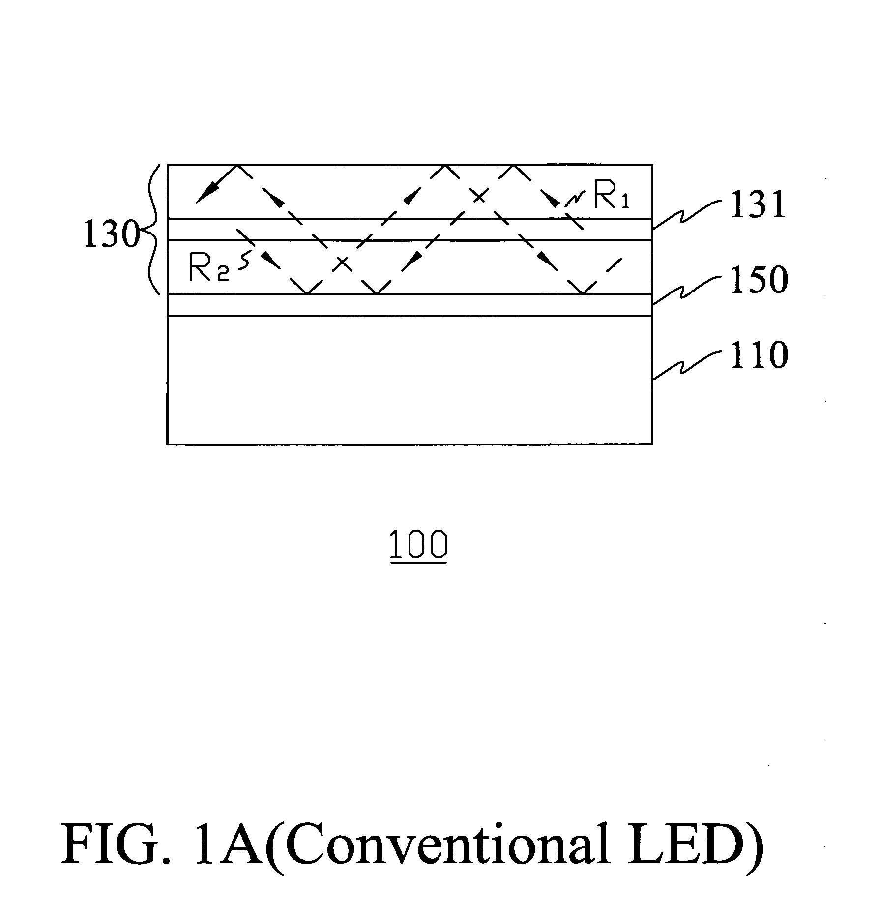
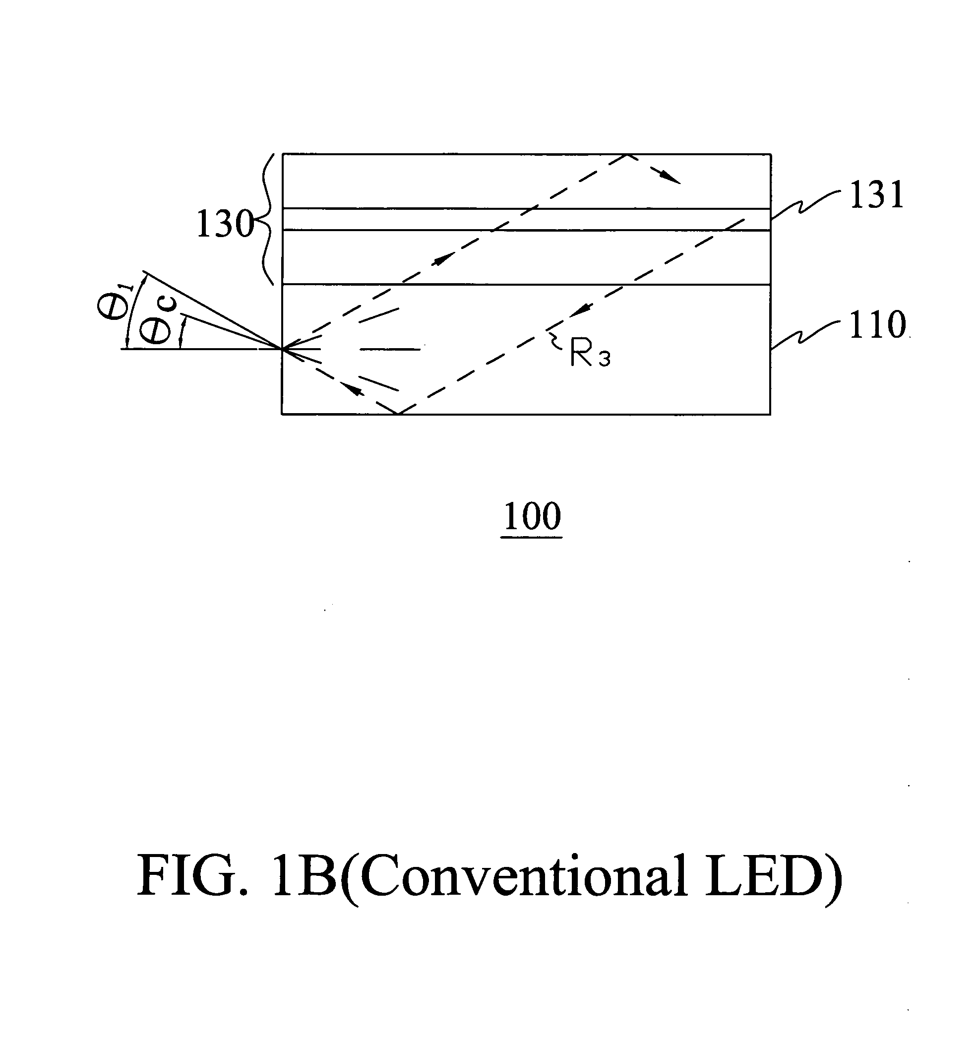
Besides, the difference of the refractive indices between the LED's material and environmental medium can result in total reflection of the light emitting to the boundary of the LED in a specific incident angle.
In general, it is unavoidable for each kind of the reflective light mentioned above to travel through inside the LED.
Because the thermal resistance of the transparent substrate 110 is usually higher, it is difficult for an LED to dissipate the heat.

Method used


Image

  • Semiconductor light emitting device
  • Semiconductor light emitting device
  • Semiconductor light emitting device

Examples


Embodiment Construction

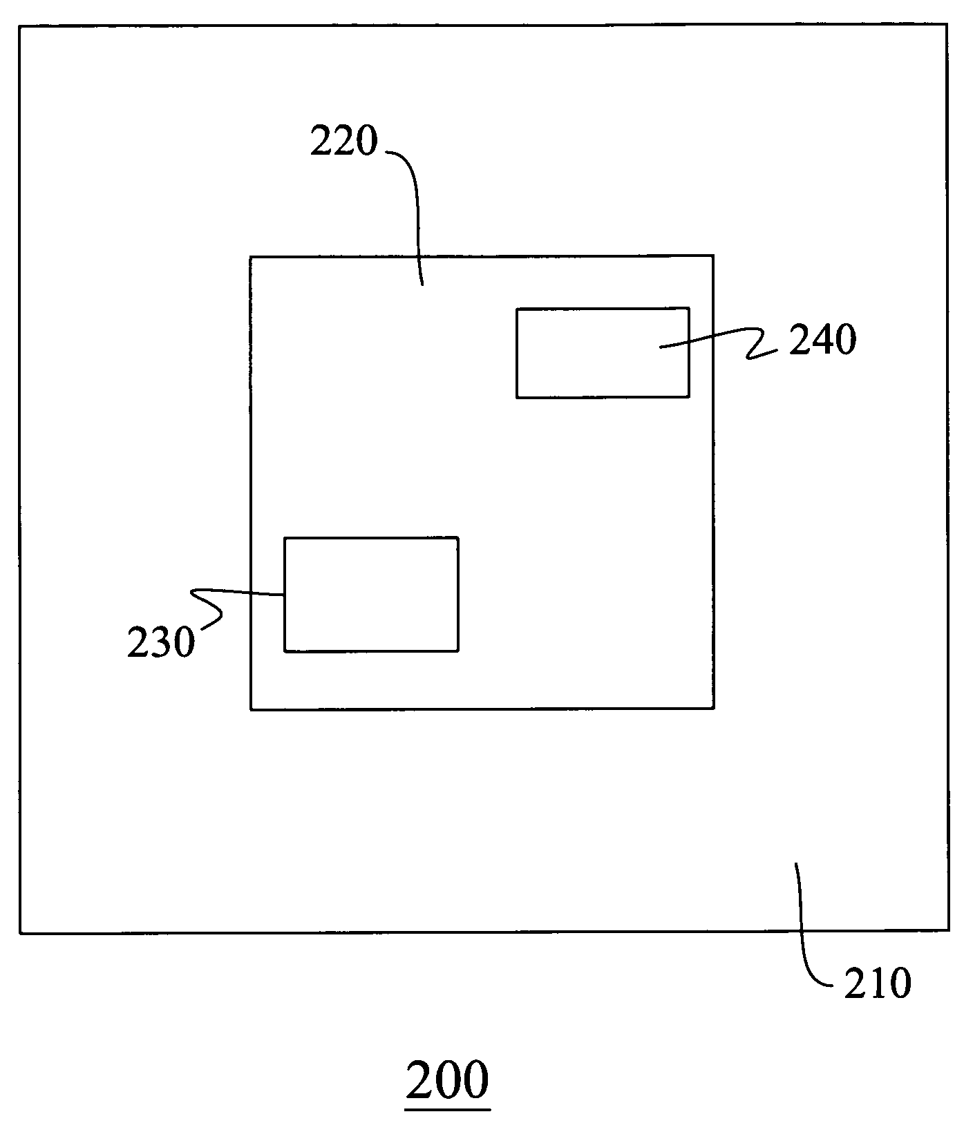
[0028]Referring to FIGS. 2A˜2B, a semiconductor light-emitting device 200 includes an external optical element 210 and a light-emitting structure 220. The light-emitting structure 220 such as an LED chip includes a semiconductor stack 221 and a transparent substrate 222, wherein the semiconductor stack 221 includes an active layer 223. When a forward voltage is applied to the light-emitting structure 220, the active layer 223 emits light. The external optical element 210 surrounds the light-emitting structure 220, connects thereto by its inner wall, and exposes at least a portion of a top surface or a bottom surface of the light-emitting structure 220. The bottom of the light-emitting structure 220 contacts with the environmental medium or a heat dissipation material (not shown here) for improving heat dissipation by thermal convection and thermal conduction. The external optical element 210 can be formed simultaneously during the manufacturing process of the light-emitting structur...


PUM


Abstract

This invention discloses a light emitting semiconductor device including a light-emitting structure and an external optical element. The optical element couples to the light-emitting structure circumferentially. In addition, the refractive index of the external optical element is greater than or about the same as that of a transparent substrate of the light-emitting structure, or in-between that of the transparent substrate and the encapsulant material.

Description

REFERENCE TO RELATED APPLICATION[0001]The present application claims the right of priority based on Taiwan Application Serial Number 096120457, filed on Jun. 6, 2007, the disclosure of which is incorporated herein by reference in its entirety.TECHNICAL FIELD[0002]The present disclosure relates to a semiconductor light-emitting device, and more particularly, to a semiconductor light-emitting device including an external optical element. The refractive index of the external optical element is larger than or about the same as that of a transparent substrate of a light-emitting structure, or in-between that of the transparent substrate and an encapsulant.BACKGROUND[0003]A light emitting diode (LED) is a solid-state semiconductor element including at least a p-n junction. The p-n junction is formed between a p-type and an n-type semiconductor layers. When the p-n junction receives a suitable forward voltage, the holes of the p-type semiconductor layer and the electrons of the n-type semi...

Claims


Application Information

Patent Timeline
Patent Type & Authority Applications(United States)
IPC IPC(8): H01L33/00H01L33/54H01L33/58H01L33/60
CPCH01L33/54H01L33/58H01L33/60H01L2933/0091
Inventor HSIEH, MIN-HSUN
Owner EPISTAR CORP
Learn More