Semiconductor device

Inactive Publication Date: 2008-12-11
RENESAS ELECTRONICS CORP
View PDF2 Cites 10 Cited by
  • Summary
  • Abstract
  • Description
  • Claims
  • Application Information

AI Technical Summary

Benefits of technology

[0015]The present invention has been accomplished in view of the above-mentioned problem and it is an object of the invention to provide a semiconductor device capable of suppressing the deterioration in reliability of the device caused by liquid soaking into a cavity.
[0017]According to the semiconductor device of this embodiment, the second spacing, i.e., the distance between adjacent gate wiring portion and contact pad portion, is 2.1 times or less as large as the first spacing, i.e., the distance between adjacent gate wiring portions. Consequently, it is possible to diminish the difference in closure shape between the gap formed between adjacent gate wiring portions and the gap formed between adjacent gate wiring portion and contact pad portion. As a result, it is possible to diminish variations in moisture resistance of the gaps and there no longer occurs penetration of liquid into a specific gap of a low moisture resistance in the wet process. Thus, it is possible to prevent the deterioration in reliability of the semiconductor device caused for example by the corrosion of wiring.

Problems solved by technology

In this patent literature, however, no consideration is given to the cavity between the wiring portion and the contact pad portion.
Thus, there has been the problem that there occurs corrosion of wiring, with consequent deterioration in reliability of the semiconductor device concerned.

Method used


Image

  • Semiconductor device
  • Semiconductor device
  • Semiconductor device

Examples


first embodiment

[0051]In this first embodiment reference will be made to a flash memory of AG-AND type as an example.

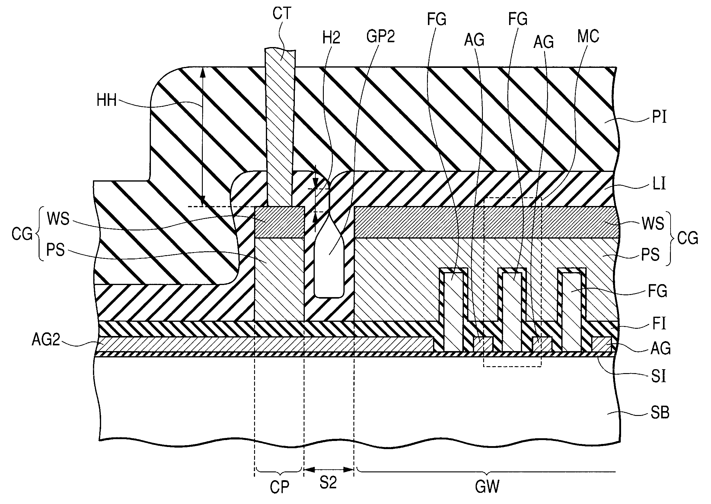
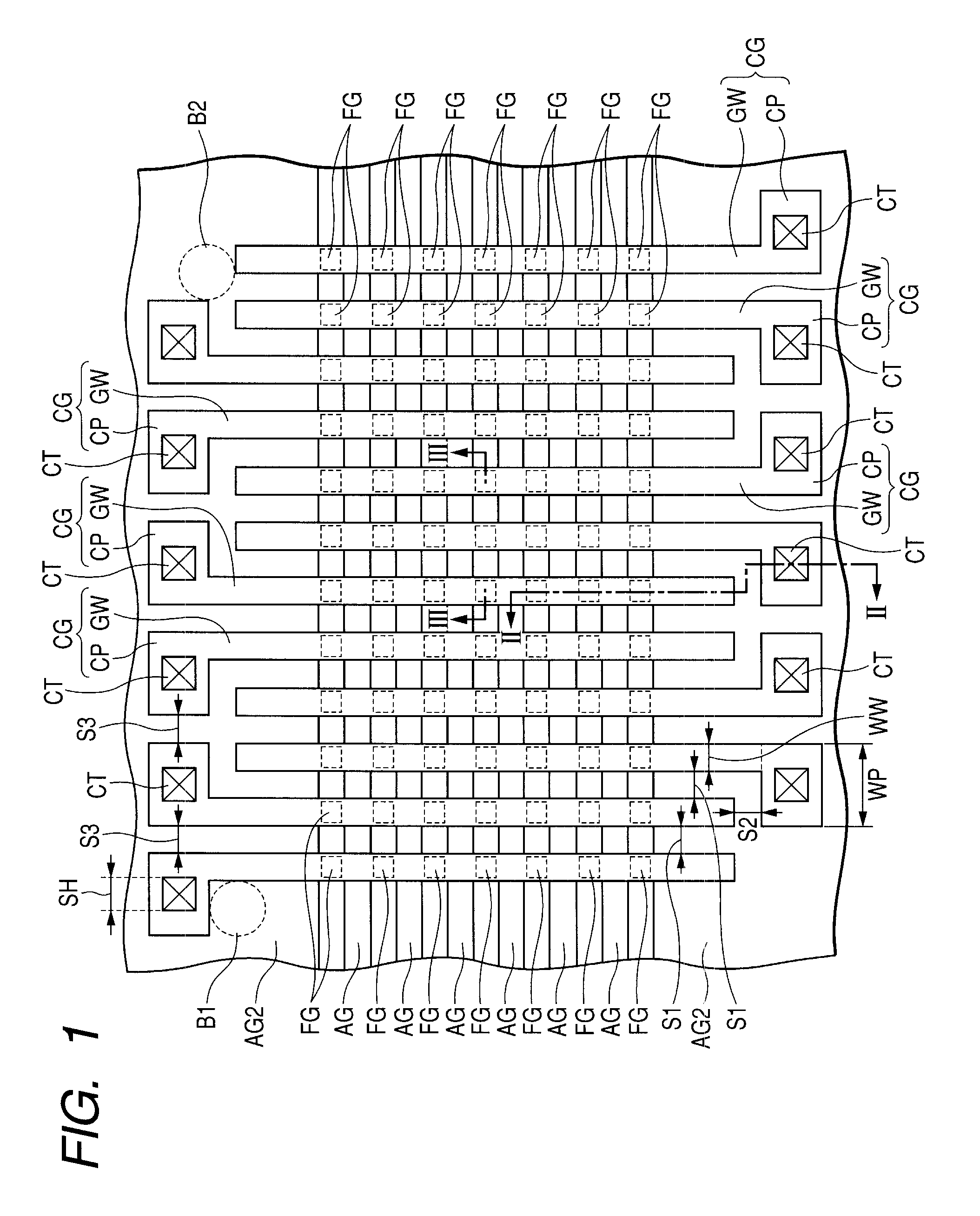
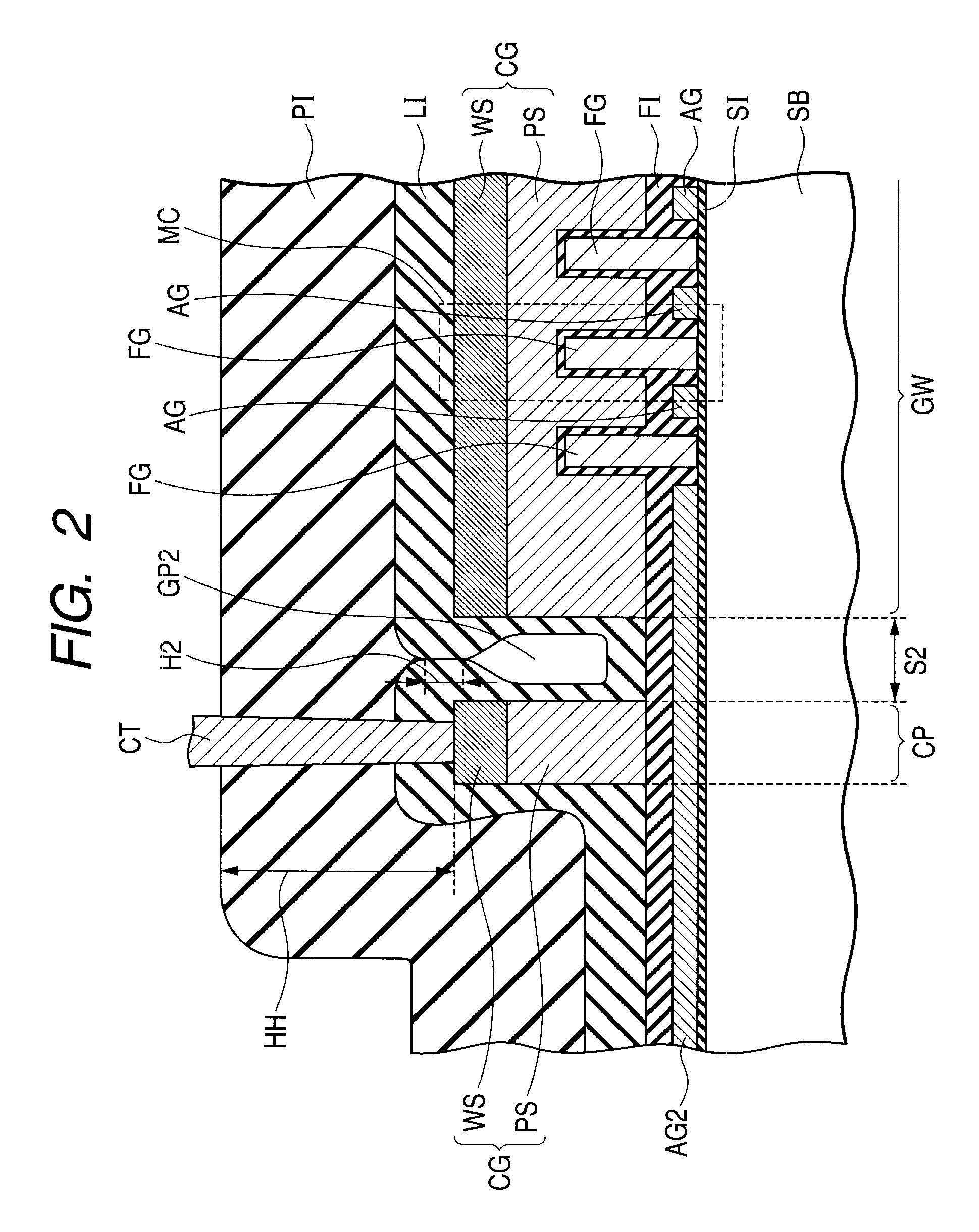
[0052]FIG. 1 is a plan view showing schematically the construction of a semiconductor device according to a first embodiment of the present invention. FIGS. 2 and 3 are schematic sectional views taken along lines II-II and III-III, respectively, in FIG. 1.

[0053]Referring mainly to FIG. 1, on a main surface of a semiconductor substrate SB formed of silicon for example, there are formed plural control gates (gate electrode layers) CG so as to extend side by side in the same direction (vertical direction in the figure) in a planar layout, and plural assist gates AG are formed side by side so as to perpendicularly intersect the control gates CG. Floating gates (floating gate electrode layers) FG are formed below the control gates CG each in an area sandwiched in between adjacent assist gates AG.

[0054]In a planar layout, each control gate CG has a gate wiring portion GW and a contact pad ...

second embodiment

[0087]Referring to FIG. 1, in this second embodiment each control gate CG is formed in such a manner that the spacing dimensions S1 and S2 become equal to each other.

[0088]Further, each control gate CG is formed in such a manner that the spacing dimensions S1 and S3 become equal to each other.

[0089]Gaps GP1 and GP2 are each formed in the position of the pattern gap portion of each control gate CG, but since the spacing dimensions S1 and S2 are equal to each other, the dimension of the gap GP1 and that of the gap GP2 are equal to each other. As a result, the gaps GP1 and GP2 are closed in similar shapes, so that the height dimension H1 of the closed portion of the gap GP1 and the height dimension H2 of the closed portion of the gap GP2 are equal to each other.

[0090]According to this second embodiment, the spacing dimension S2 (FIG. 2) between the gate wiring portion GW and the contact pad portion CP and the spacing dimension S1 (FIG. 3) between adjacent gate wiring portions GW are ma...

third embodiment

[0094]FIG. 12 is a plan view showing schematically a planar layout of gate electrode layers (control gates) in a third embodiment of the present invention.

[0095]A planar layout of control gates CG in this third embodiment corresponds to a pattern of a shape obtained by removing band-like patterns of width dimensions S1, S2 and S3 from a minimum rectangular pattern including all of plural control gates CG.

[0096]The control gates CG are formed in such a manner that adjacent contact pad portions CP project in the same direction with respect to the gate wiring portions GW.

[0097]Other constructional points of this third embodiment are almost the same as in the construction of the previous first or second embodiment. Therefore, the same elements as in the previous first or second embodiment are identified by the same reference numerals as in the previous embodiment and explanations thereof will here be omitted.

[0098]Next, a description will be given about the difference in point of effect...


PUM


Abstract

A semiconductor device is provided which can suppress the deterioration of its reliability caused by liquid soaking into a gap. The semiconductor device includes plural gate electrode layers and an interlayer insulating film. The gate electrode layers are formed so as to extend in the same direction in a planar layout and each have a gate wiring portion and a contact pad portion. The interlayer insulating film is formed over the gate electrode layers and gaps so as to leave the gaps each between adjacent gate wiring portions and also between adjacent gate wiring portion and contact pad portion. A second spacing which is the distance between adjacent gate wiring portion and contact pad portion is 2.1 times or less as large as a first spacing which is the distance between adjacent gate wiring portions.

Description

CROSS-REFERENCE TO RELATED APPLICATIONS [0001]The disclosure of Japanese Patent Application No. 2007-152752 filed on Jun. 8, 2007 including the specification, drawings and abstract is incorporated herein by reference in its entirety.BACKGROUND OF THE INVENTION[0002]The present invention relates to a semiconductor device and more particularly to a semiconductor device having a gap portion between gates.[0003]Reduction of size and microfabrication of semiconductor memories have been being performed, and as to the layout of transistor gate wiring within a memory array, a layout based on a minimum design rule (L / S (Line and Space) rule is adopted in many cases. At an end of the wiring layout thus based on the minimum L / S rule there is provided a contact pattern (contact pad portion) for electric connection with the wiring (see, for example, Patent Literature 1).[0004]As a semiconductor memory having gate wiring there is known, for example, a flash memory of AG-AND (Assist Gate-AND) type...

Claims


Application Information

Patent Timeline
IPC IPC(8): H01L23/538
CPCH01L27/11519H01L27/11521H10B41/10H10B41/30H01L29/66477H10B63/80
Inventor YONEMOCHI, YASUAKIOTOI, HISAKAZU
Owner RENESAS ELECTRONICS CORP
Why Eureka
Try Eureka