Control circuit for a high-side semiconductor switch for switching a supply voltage

a control circuit and semiconductor switch technology, applied in the direction of electronic switching, semiconductor devices, pulse techniques, etc., can solve the problems of high price compared to a purely discrete circuit, additional functionalities, and complex individual function blocks in these ics, and achieve the effect of reliably maintaining the stationary off state and minimizing losses

Inactive Publication Date: 2008-12-11
MINEBEA CO LTD
View PDF1 Cites 15 Cited by
  • Summary
  • Abstract
  • Description
  • Claims
  • Application Information

AI Technical Summary

Benefits of technology

[0019]Different resistance values as current negative feedback may thereby be set for the control semiconductor switch, in order, depending on the switching and current supply state of the high-side semiconductor switch, to minimize losses in the control semiconductor switch, or to reliably maintain the stationary OFF state of the high-side semiconductor switch.

Problems solved by technology

However, the individual function blocks in these ICs are distinctly more complex than as described above and the ICs generally have additional functionalities.
The disadvantage is the high price compared to a purely discrete circuit.
For discretely constructed high-side control circuits, there are often difficulties for motor applications in the region of the level shift circuit that are not acceptable.
In the case of a high-active control, it is thus necessary to conduct a current to ground during the ON time of the high-side semiconductor switch, which, for high supply voltages, results in considerable losses and associated component heating.
For low-active control circuits, a similar problem arises during switch-off of the high-side semiconductor switch when it directs a current in the reverse direction (reverse current) through its inverse diode, as can happen in motor applications when, after commutation, an electric motor in generator mode feeds back current into the control circuit for a short time.

Method used


Image

  • Control circuit for a high-side semiconductor switch for switching a supply voltage
  • Control circuit for a high-side semiconductor switch for switching a supply voltage
  • Control circuit for a high-side semiconductor switch for switching a supply voltage

Examples


Embodiment Construction

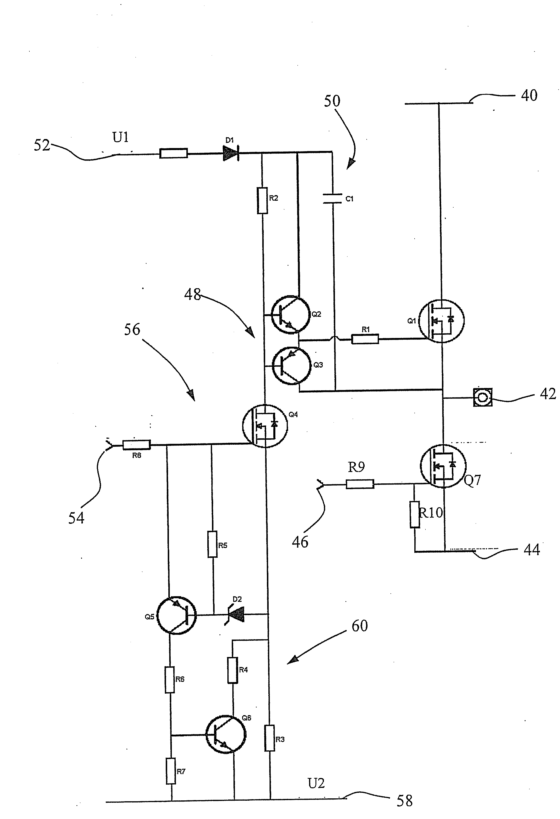
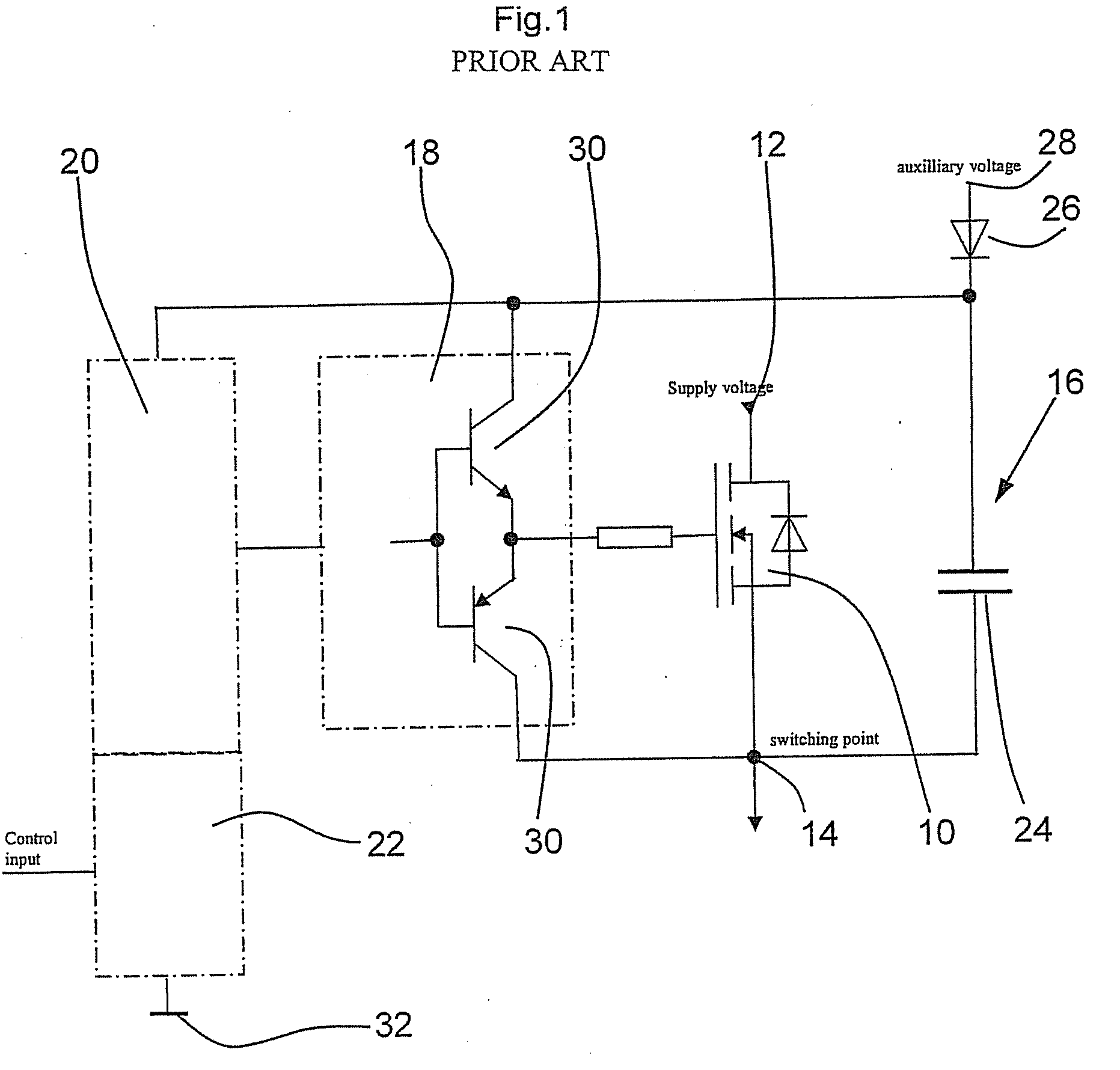
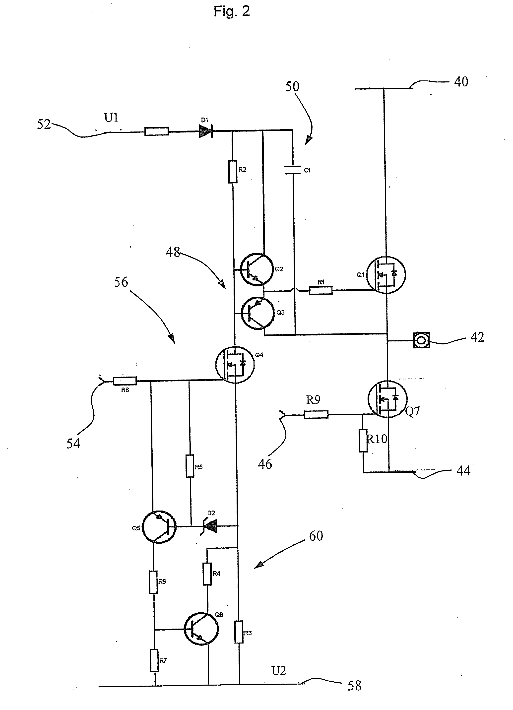
[0036]FIG. 2 shows a circuit diagram of a control circuit for a high-side semiconductor switch according to the invention. The circuit of FIG. 2 is basically constructed with the same function blocks that are shown in FIG. 1. The circuit portion for providing the drive voltage for the high-side semiconductor switch and the driver circuit in the illustrated embodiment are constructed in the same way as in the prior art. It is not always possible to unequivocally allocate every component to the respective function blocks; the boundary between two function blocks could more or less run “straight through” a component. In particular, the boundary between the input circuit portion, which receives the ground-related control signal, and the level shift circuit signal, which transforms this control signal into a floating voltage level for the driver circuit, can not be unequivocally drawn.

[0037]The embodiment illustrated in FIG. 2 of the control circuit comprises the following components: a ...


PUM


Abstract

A high-side semiconductor switch control circuit for switching a positive supply voltage is provided, having a circuit to provide a drive voltage for the high-side semiconductor switch, a driver circuit for driving the high-side semiconductor switch based on the control circuit, wherein both the circuit for providing the drive voltage as well as the driver circuit operate in relation to a floating switching point, an input circuit portion that receives a control signal related to ground, and a level shift circuit portion that is connected between the input circuit portion and the driver circuit portion and set up so as to transform the control signal related to ground into a floating voltage level for the driver circuit portion.

Description

FIELD OF THE INVENTION[0001]The invention relates to a control circuit for a high-side semiconductor switch for switching a supply voltage.BACKGROUND OF THE INVENTION[0002]High-side semiconductor switches are semiconductor switches that can switch a high supply voltage of several 100 V, such as 320 V direct current voltage. To this effect, they are connected between a positive supply voltage and a floating switching point, which, during switching operations, passes through a voltage range from ground potential to a potential close to the positive supply voltage. High-side semiconductor switches are used, for example, for driving electric motors at the mains voltage or in buck converters. They are generally realized as power transistors, such as MOSFETs (metal oxide field effect transistors) and IGBTs (bipolar transistors with insulated gate electrodes).[0003]Control circuits for high-side semiconductor switches, referred to below in short as high-side control circuits, are described...

Claims


Application Information

Patent Timeline
Patent Type & Authority Applications(United States)
IPC IPC(8): H03K17/16
CPCH03K17/063H03K17/08142H03K17/567H03K17/6872H03K2017/066H03K2217/0036
Inventor STEGMAYR, THOMAS
Owner MINEBEA CO LTD
Why Eureka
Try Eureka