
Optical element and projection display device

a technology of optical elements and projection display devices, which is applied in the direction of projectors, polarising elements, instruments, etc., can solve the problems of reducing the lifetime or unstable operation of the liquid crystal device, and the instability of fine wires arranged in the vicinity of the steps, so as to reduce the diffusion effect of transmitted light and maximize the diffusion effect of reflected ligh

Active Publication Date: 2008-12-11
SEIKO EPSON CORP
View PDF3 Cites 22 Cited by
  • Summary
  • Abstract
  • Description
  • Claims
  • Application Information

AI Technical Summary

Benefits of technology

[0008]An advantage of the invention is to provide an optical element having a reflected light diffusing function and a polarization separation function.
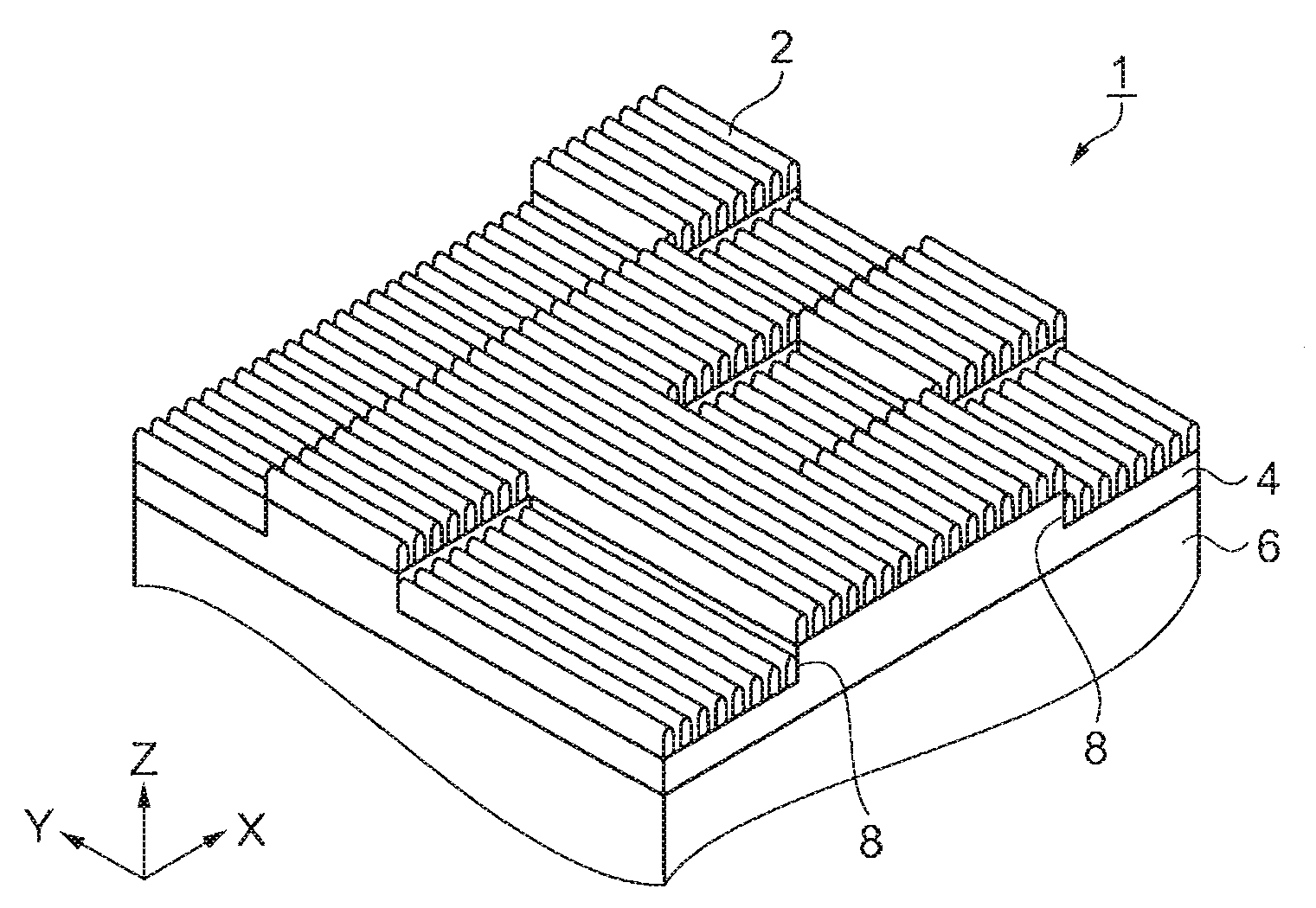
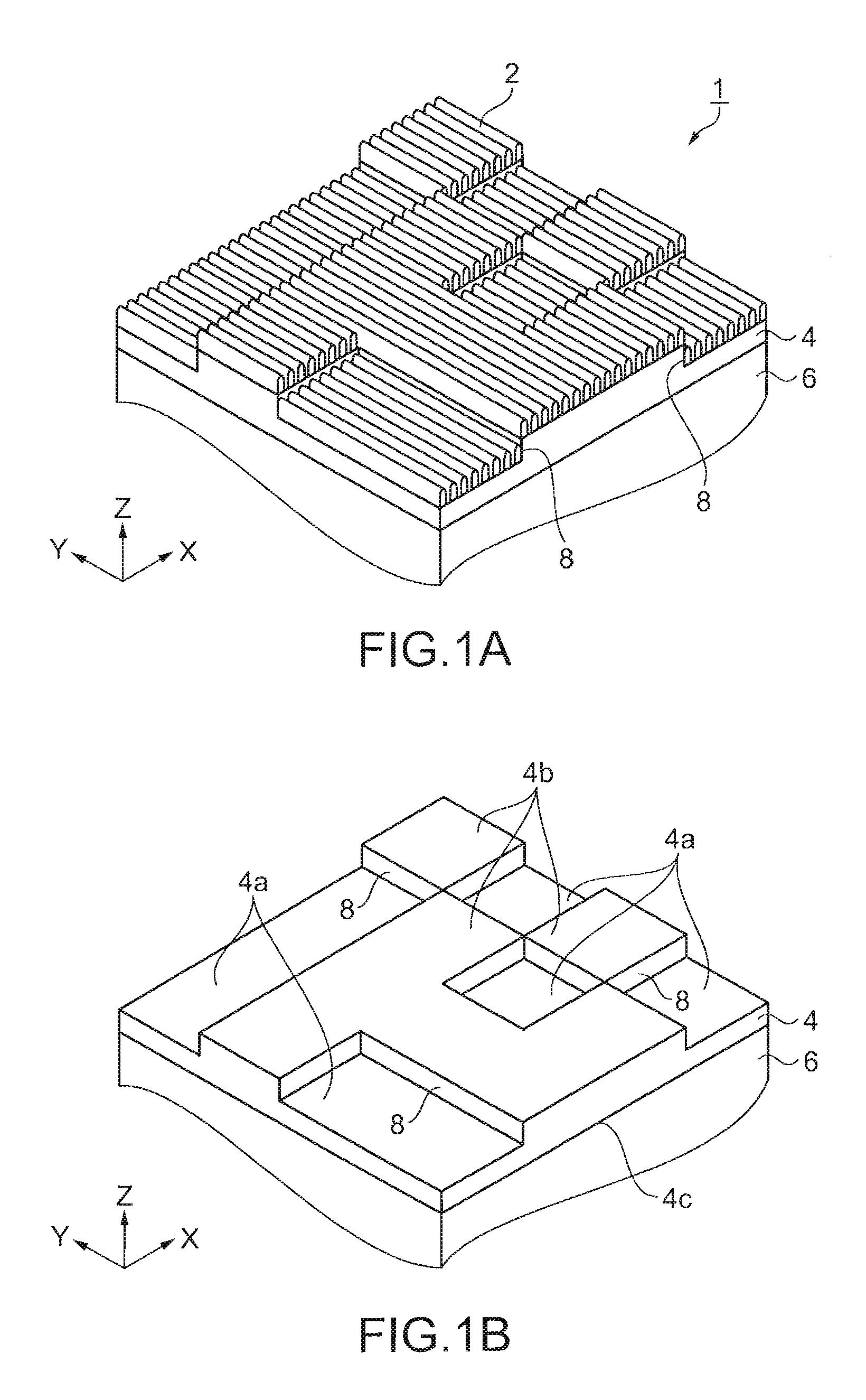
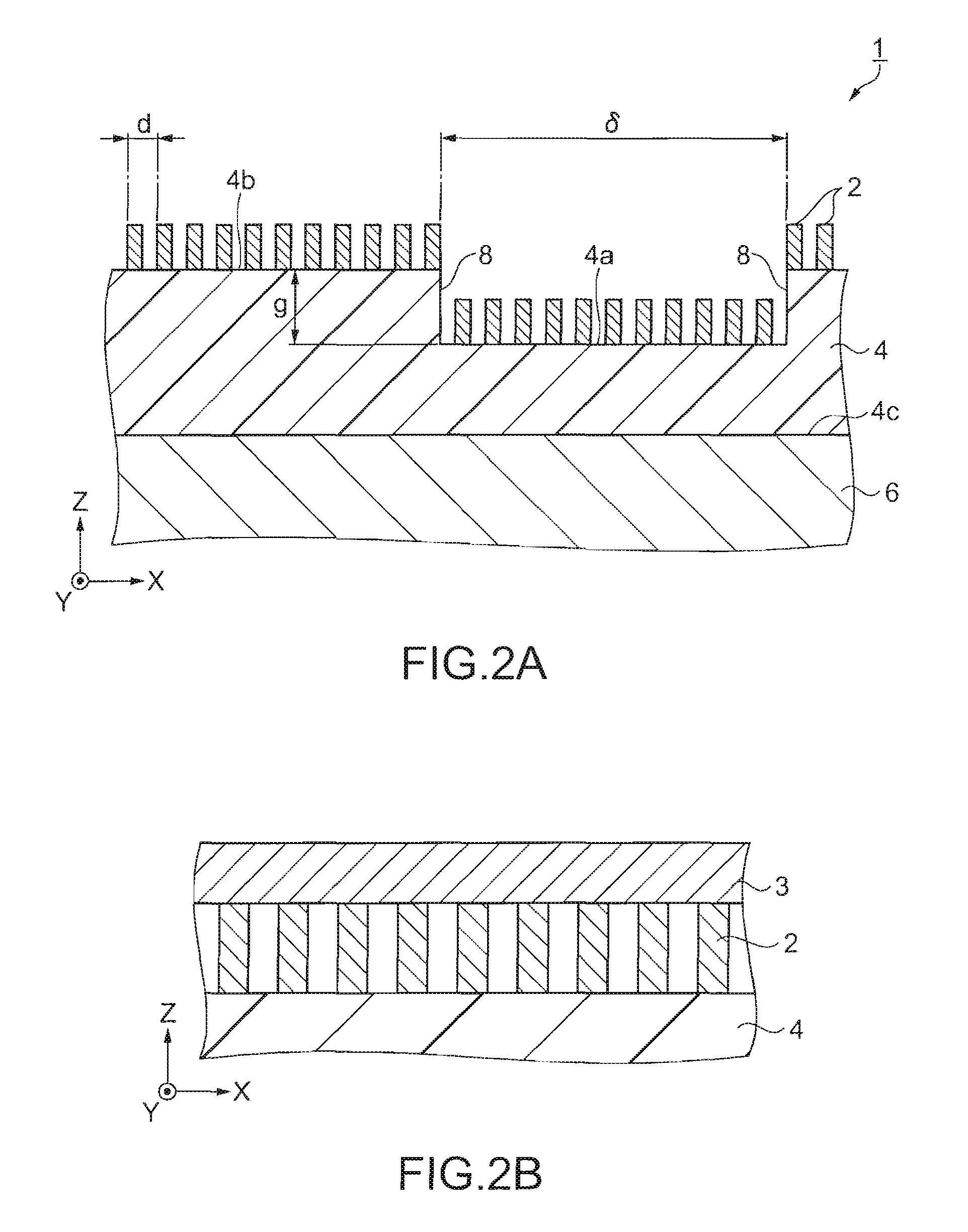
[0009]According to a first aspect of the invention, an optical element includes a diffractive functional layer which diffracts at least part of incident light, and a grid formed on a first surface of the diffractive functional layer, the grid including a plurality of fine wires and having a polarization separation function. Here, the optical element reflects a part of the incident light while transmitting another part of the incident light, and the first surface of the diffractive functional layer includes a plurality of first regions, a plurality of second regions, and a step provided at a border between the first regions and the second regions. The height of the plurality of second regions relative to a second surface of the diffractive functional layer is different from that of the first regions, and the second surface is a surface opposite to the first surface.
[0010]In this structure, a plurality of relief patterns composed of the first regions and the second regions is distributed on the first surface of the diffractive functional layer. The distribution of relief patterns allows the diffractive functional layer to diffract the incident light, so that the light is diffused to directions different from the direction of incidence.
[0011]An incident light component that has a polarization axis parallel to the fine wires is reflected at the grid, and another component that has a polarization axis orthogonal to the fine wires is transmitted. Consequently, with the optical element, the incident light beam is separated into a reflected light beam and a transmitted light beam, and the reflected light beam is diffused out.
[0012]In this case, the height relative to the second surface in the first regions of the optical element may be different from that of the second regions by (2m+1)λ / 4n, where m being an integer greater than or equal to 0, λ being a wavelength of the incident light, and n being a refraction index of the medium over the optical element.
[0013]In this structure, the height difference of the first regions and the second regions being (2m+1)λ / 4n maximizes the diffusion effect of the reflected light by the diffractive functional layer. Since the diffusion effect of the transmitted light is not necessarily the highest at this point, the intensity of 0th order diffraction light of the light transmitted through the diffractive functional layer stays almost intact while reducing the diffusion effects on the transmitted light. Consequently, with the optical element, the incident light beam is separated into a reflected light beam and a transmitted light beam, and at the same time, the reflected light is diffused out while the transmitted light is not.

Problems solved by technology

This results in problems of the reduced lifetime or unstable operation of the liquid crystal device 10.
This structure makes the fine wires unparallel to the step provided at the border between the first regions and the second regions, thereby avoiding defects in which the fine wires arranged in the vicinity of the steps become unstable.

Method used


Image

  • Optical element and projection display device
  • Optical element and projection display device
  • Optical element and projection display device

Examples


first modification

[0108]As described above, according to the optical element 1, the diffractive functional layer 4 provides the reflected light 80r with an appropriate intensity distribution and range. Here, a spatial intensity distribution of the reflected light 80r is controlled in accordance with the shape or the size of the liquid crystal device 10, by improving either an order of an alignment of the concaves and convexes of the diffractive functional layer 4 (i.e. the arrangement of the first regions 4a and the second regions 4b) or a planer shape thereof. In other words, the reflected light 80r can be collected to a specific location.

[0109]For instance, the shapes of the first regions 4a and the second regions 4b in the diffractive functional layer 4 are not limited to the ones illustrated in FIGS. 1A, 1B, and 3A, but may also include the shape illustrated in FIG. 13. Referring to FIG. 13, the black regions are equivalent to the first regions 4a , and the white regions are equivalent to the sec...

second modification

[0114]The projector 100 may have a structure in which a plurality of liquid crystal devices 10 is used. FIG. 16 is a schematic drawing illustrating an optical system of the projector 100 provided with three liquid crystal devices 10. This optical system includes a prism 53 provided with four planes, the optical element 1 arranged to face one of the planes of the prism 53, and the liquid crystal devices 10R, 10G, and 10B arranged so as to respectively face the other three planes of the prism 53. The prism 53 refracts light beams entering from the liquid crystal devices 10R, 10G, and 10B, and enters the light beams into the optical element 1. That is to say, the prism 53 is arranged in the optical paths reaching the optical element 1 from each of the liquid crystal devices 10R, 10G, and 10B. The liquid crystal devices 10R, 10G, and 10B respectively modulate the intensity of red, green, and blue light beams. Display light is obtained by synthesizing the intensity-modulated light beams ...

third modification

[0120]A substance with a refraction index larger than 1 may be deposited on the side of the grid 2 in the optical element 1. FIG. 18 is a sectional drawing illustrating a state in which a SiN layer is deposited on the optical device 1. Illustration of the sealing layer 3 (FIG. 1B) is omitted in FIG. 18.

[0121]When controlling the diffusion effect of the optical element 1, the optimal value of the height g of the steps 8 in the diffractive functional layer 4 depends on a refraction index n of the surrounding media, as explained in formula (1). For instance, if SiN (n≈1.5) is used as the surrounding media as illustrated in FIG. 18, the height g is reduced compared to the case of the surrounding media such as air (n≈1.0). The smaller the height g of the steps 8, the manufacturing processes of the grid 2 including photolithography become easier, allowing the easier manufacturing of the grid 2.

Forth Modification

[0122]A field lens 52 may be arranged as a collective lens at an optional posi...


PUM


Abstract

An optical element, includes: a diffractive functional layer which diffracts at least part of incident light; and a grid formed on a first surface of the diffractive functional layer, the grid including a plurality of fine wires and having a polarization separation function; wherein the optical element reflects a part of the incident light while transmitting another part of the incident light, the first surface of the diffractive functional layer including a plurality of first regions; a plurality of second regions, a height thereof relative to a second surface of the diffractive functional layer being different from that of the first regions, the second surface being an opposite surface to the first surface; and a step provided at a border between the first regions and the second regions.

Description

[0001]The entire disclosure of Japanese Patent Application Nos: 2007-151225, filed Jun. 7, 2007 and 2008-118149, filed Apr. 30, 2008 are expressly incorporated by reference herein,BACKGROUND[0002]1. Technical Field[0003]Several aspects of the present invention relate to an optical element as well as to a projection display device.[0004]2. Related Art[0005]Wire-grid polarizers are known as one of the optical elements provided with a polarization separation function. These wire-grid polarizers have multiple conductive fine wires arranged at a pitch shorter than the wavelength of light, and they reflect an incident light component that has a polarization axis parallel to the fine wires, while transmitting another component that has a polarization axis orthogonal to the fine wires.[0006]Wire-grid polarizers are formed of an inorganic substance and therefore excel in light resistance. For this reason, there are attempts to apply these wire-grid polarizers to projection display devices su...

Claims


Application Information

Patent Timeline
IPC IPC(8): G02B5/18G02B5/30
CPCG02B5/1842G02B5/1861G02B5/3058
Inventor AMAKO, JUNSAWAKI, DAISUKE
Owner SEIKO EPSON CORP
Learn More