Method for forming polycrystalline thin film bipolar transistors

a technology of bipolar transistors and polysilicon films, which is applied in the direction of electrical equipment, semiconductor devices, instruments, etc., can solve the problems of low carrier lifetime and high defect densities of polysilicon films

Active Publication Date: 2008-12-18
SANDISK TECH LLC
View PDF28 Cites 81 Cited by
  • Summary
  • Abstract
  • Description
  • Claims
  • Application Information

AI Technical Summary

Benefits of technology

[0008]Another aspect of the invention provides for a method for forming a memory select device comprising the steps: monolithically forming a first memory level of first memory cells above a substrate, each first memory cell comprising a vertically oriented p-i-n diode, the cells being arranged in rows and columns within the first memory level; and forming one or more first bipolar transistor in operative connection to and substantially coplanar with the first memory cells, wherein the first memory cells and the first bipolar transistors comprise deposited semiconductor material crystallized in contact with cobalt silicide or titanium silicide, and wherein the first bipolar transistors are capable of selectively programming one or more of the first memory cells. Additional memory levels may be monolithically formed above the first memory level, with corresponding additional bipolar transistors being formed within respective memory levels in operative connection to and substantially coplanar with the memory cells of that level.

Problems solved by technology

Polycrystalline forms of silicon (“polysilicon”), germanium (“polygermanium”), and silicon germanium (“polysilicon polygermanium”) typically are not used to make bipolar transistors because usually these materials do not provide sufficient current gain for electronic applications of this type.
The polysilicon films have very high defect densities, which accounts for the low carrier lifetimes.

Method used


Image

  • Method for forming polycrystalline thin film bipolar transistors
  • Method for forming polycrystalline thin film bipolar transistors
  • Method for forming polycrystalline thin film bipolar transistors

Examples


Embodiment Construction

[0005]The present invention is defined by the following claims, and nothing in this section should be taken as a limitation on those claims.

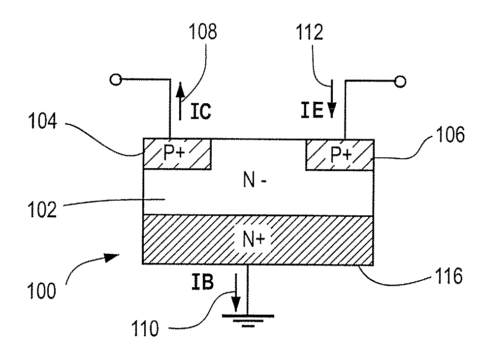
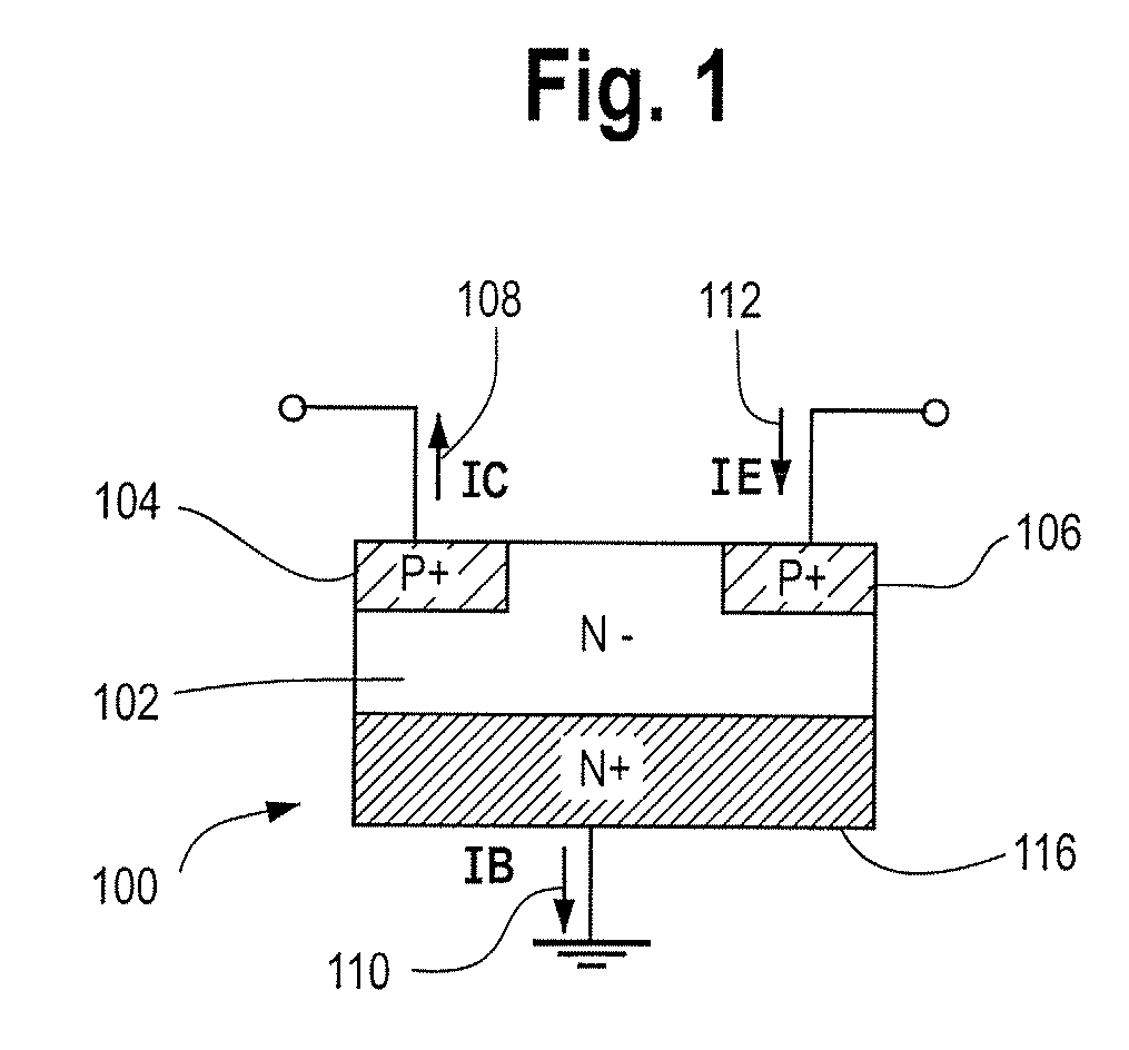
[0006]In one embodiment, the invention is directed to a method of forming a bipolar transistor comprising the steps of: depositing a layer of amorphous semiconductor material comprising silicon, germanium or silicon-germanium above a substrate; depositing a metal in contact with the amorphous semiconductor material; annealing to react the metal with the amorphous semiconductor material to form a crystallization template layer comprising metal silicide, metal germanide or metal silicide-germanide and to crystallize the layer of semiconductor material. The crystallization template layer preferably comprises titanium silicide, germanide or silicide-germanide.

[0007]Another aspect of the invention provides for a method for making a thin film bipolar transistor comprising the steps of: depositing a layer of amorphous silicon above a substrate; doping ...


PUM

PropertyMeasurementUnit
sizeaaaaaaaaaa
diameteraaaaaaaaaa
diameteraaaaaaaaaa

Abstract

A method is described for forming a semiconductor device comprising a bipolar transistor having a base region, an emitter region and a collector region, wherein the base region comprises polycrystalline semiconductor material formed by crystallizing silicon, germanium or silicon germanium in contact with a silicide, germanide or silicide germanide. The emitter region and collector region also may be formed from polycrystalline semiconductor material formed by crystallizing silicon, germanium or silicon germanium in contact with a silicide, germanide or silicide germanide forming metal. The polycrystalline semiconductor material is preferably silicided polysilicon, which is formed in contact with C49 phase titanium silicide.

Description

CROSS-REFERENCE TO RELATED APPLICATIONS[0001]This application is related to Herner et al., U.S. patent application Ser. No. ______, entitled “Method To Form Low-Defect Polycrystalline Semiconductor Material For Use In A Transistor,” (Reference No. SAND-01198US0) and to Petti et al., U.S. patent application Ser. No. ______, entitled “Polycrystalline Thin Film Bipolar Transistors,” (Reference No. 2052 / 98694) which are being filed herewith and which are hereby incorporated by reference.BACKGROUND OF THE INVENTION[0002]Bipolar transistors typically are formed in single crystal silicon. Single crystals of other semiconductor materials, such as germanium, silicon germanium and other semiconductor materials, also are sometimes used. Polycrystalline forms of silicon (“polysilicon”), germanium (“polygermanium”), and silicon germanium (“polysilicon polygermanium”) typically are not used to make bipolar transistors because usually these materials do not provide sufficient current gain for elec...

Claims


Application Information

Patent Timeline
Patent Type & Authority Applications(United States)
IPC IPC(8): H01L21/331
CPCG11C17/16H01L29/66265H01L29/7317
Inventor PETTI, CHRISTOPHER J.HERNER, S. BRAD
Owner SANDISK TECH LLC
Why Eureka
Try Eureka