Thin double-sided package substrate and manufacture method thereof

a packaging substrate and double-sided technology, applied in the field of packaging substrates, can solve the problems of heat dissipation and impair the slimming of the chip package, and achieve the effects of promoting chip package reliability, reducing package thickness, and enhancing heat dissipation

Inactive Publication Date: 2008-12-25
GIOTEK OPTOELECTRONICS +1
View PDF2 Cites 36 Cited by
  • Summary
  • Abstract
  • Description
  • Claims
  • Application Information

AI Technical Summary

Benefits of technology

[0007]One objective of the present invention is to provide a thin double-sided package substrate and a manufacture method thereof to overcome the abovementioned problems, wherein the carrier is partially or totally removed to form a chip receiving bay accommodating a chip so as to reduce the package thickness and enhance the heat dissipation of the chip, and wherein the through-hole does not penetrate the lower conductive layer lest humidity permeate through the inner wall of the through-hole to the upper surface of the carrier, whereby the reliability of the chip package is promoted and the flexibility of the circuit layout is increased.

Problems solved by technology

Besides, the chip 21 is fixedly installed on the package substrate which not only makes worse the heat dissipation of the chip 21 but also impairs the slimming of the chip package.

Method used


Image

  • Thin double-sided package substrate and manufacture method thereof
  • Thin double-sided package substrate and manufacture method thereof
  • Thin double-sided package substrate and manufacture method thereof

Examples


Embodiment Construction

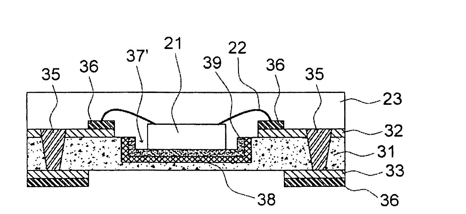
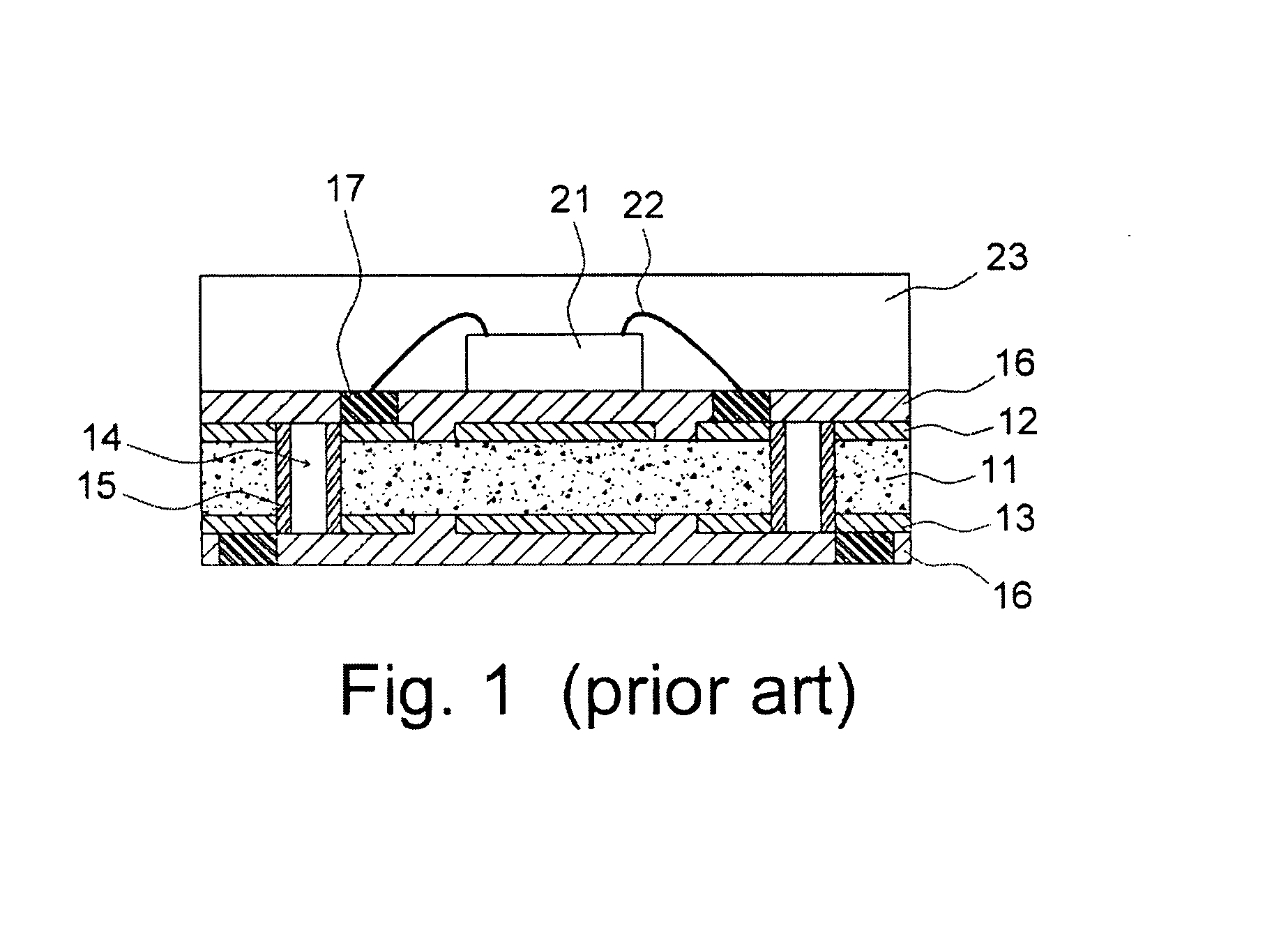
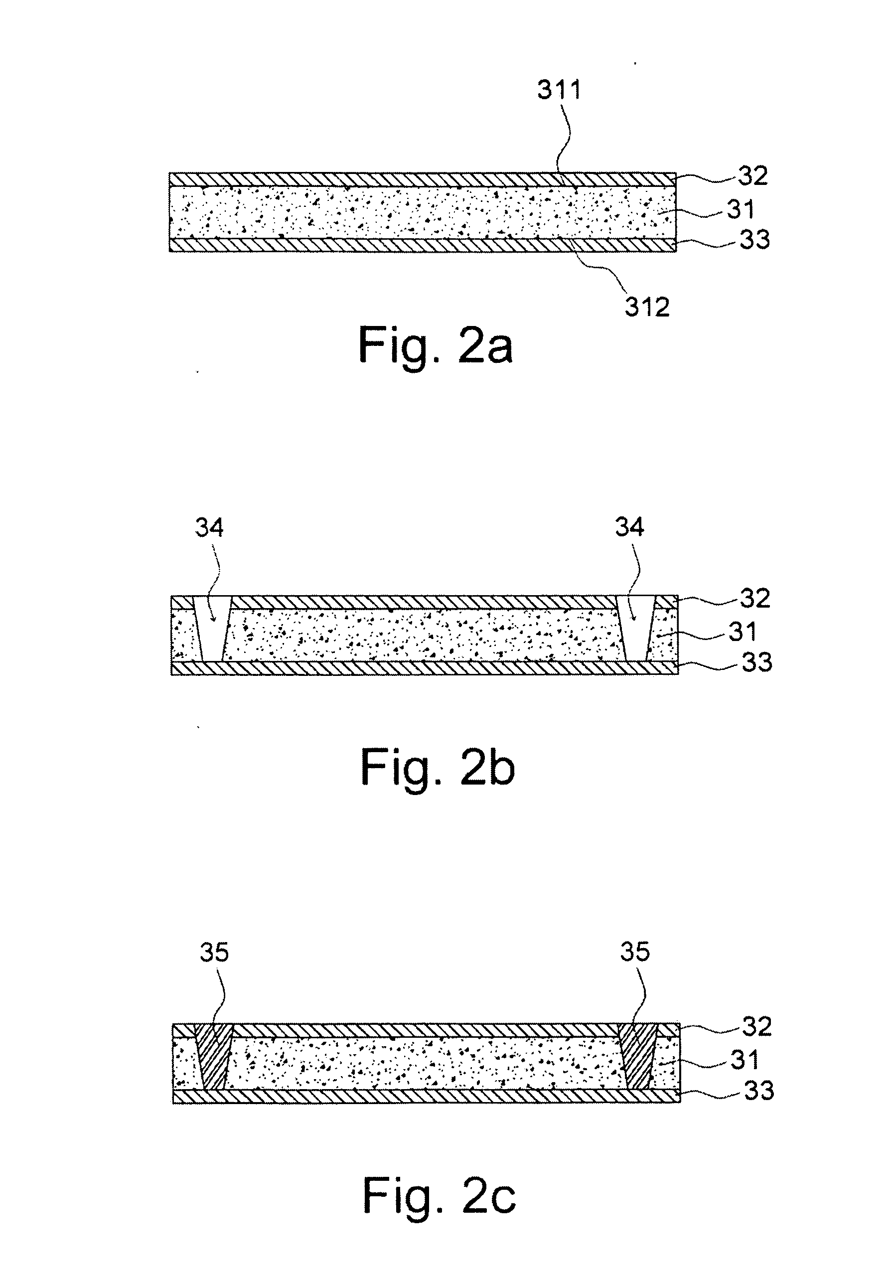
[0015]Refer to from FIG. 2a to FIG. 2f for illustrating the process of a manufacture method for a thin double-sided package substrate according to a preferred embodiment of the present invention. Refer to FIG. 2a. Firstly, a carrier 31 having a first surface 311 and a second surface 312 is provided. The carrier 31 may be made of a copper clad laminate, an insulating material, a glass fiber prepreg, or a polymeric material etc. A first conductive layer 32 and a second conductive layer 33 are respectively formed on the first surface 311 and the second surface 312. The first and second conductive layers 32 and 33 may be made of a metal, preferably copper.

[0016]Refer to FIG. 2b. A through-hole 34 penetrates the first conductive layer 32, the first and second surfaces 311 and 312 of the carrier 31. It is to be noted that the through-hole 34 does not penetrate the second conductive layer 33. Therefore, humidity will not permeate through the inner wall of the through-hole 34 to the upper l...


PUM

PropertyMeasurementUnit
conductiveaaaaaaaaaa
electricallyaaaaaaaaaa
insulatingaaaaaaaaaa

Abstract

The present invention discloses a manufacture method for a thin double-sided package substrate, which includes steps: providing a carrier; respectively forming a first conductive layer and a second conductive layer on the upper and lower surfaces of the carrier; forming a through-hole penetrating the first conductive layer and the carrier but not penetrating the second conductive layer; setting a conductive element in the through-hole to electrically connect the first conductive layer with the second conductive layer; forming desired circuits on the first conductive layer and / or the second conductive layer; forming a first metal layer on the first conductive layer and / or the second conductive layer; and removing the carrier located in a predetermined region to form a chip receiving bay. The present invention also discloses a package substrate made by the abovementioned manufacture method, which can reduce the overall thickness of a chip package structure, increase the heat-dissipation effect of the chip and prevent the chip package structure from humidity penetration.

Description

BACKGROUND OF THE INVENTION[0001]1. Field of the Invention[0002]The present invention relates to a package substrate and a manufacture method thereof, particularly to a thin double-sided package substrate and a manufacture method thereof[0003]2. Description of the Related Art[0004]Refer to FIG. 1 In a conventional package substrate having circuits on both sides thereof, conductive layers 11 and 12 are respectively formed on the upper and lower surfaces of a carrier 11, and the desired circuits are formed on the conductive layers 11 and 12. A through-hole 14 penetrates the carrier 11, and a conductive element 15 is set inside the through-hole 14 to electrically connect the conductive layer 12 with the conductive layer 13. Besides, an insulating material, such as a resin or a solder mask, may further be filled into the through-hole 14. A metal finishing process is used to form a solder pad 17. A solder mask layer 16 is formed oil the conductive layers 12 and 13 with the solder pad 17 ...

Claims


Application Information

Patent Timeline
Patent Type & Authority Applications(United States)
IPC IPC(8): H01L33/00H01L23/48H05K3/42H01L33/48H01L33/60
CPCH01L21/486H01L2224/85H01L23/3735H01L23/49822H01L23/49827H01L24/83H01L24/85H01L33/486H01L33/60H01L2224/48091H01L2224/83801H01L2924/01046H01L2924/01078H01L2924/01079H01L2924/15153H01L2924/15165H01L2924/1517Y10T29/49165H01L2924/00011H01L24/48H01L2224/32225H01L2224/48227H01L2224/73265H01L23/13H01L2924/00014H01L2924/00H01L2924/00012H01L2224/83851H01L24/73H01L2924/12041H01L2924/181H01L2224/45099H01L2224/45015H01L2924/207
Inventor LIN, CHI CHIHSUN, BOWANG, HUNG JENTSENG, JEN FENG
Owner GIOTEK OPTOELECTRONICS
Why Eureka
Try Eureka