

Fin field effect transistor devices with self-aligned source and drain regions
a technology of fin field effect transistor and drain region, which is applied in the direction of semiconductor devices, electrical devices, nanotechnology, etc., can solve the problems of difficult alignment of landing pads with gate, significant fabrication challenges, and difficulty in contacting source and drain
- Summary
- Abstract
- Description
- Claims
- Application Information
AI Technical Summary
Benefits of technology
Problems solved by technology
Method used
Image

Examples
Embodiment Construction
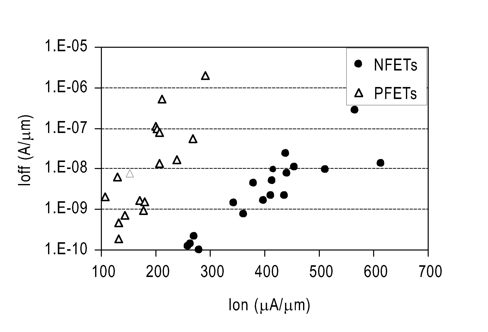
[0028]FIGS. 1A-O are diagrams illustrating exemplary methodology 100 for fabricating a fin field effect transistor (FinFET) device. As will be described in detail below, the present techniques make use of a damascene gate process to construct source / drain regions that are self-aligned with the gate.
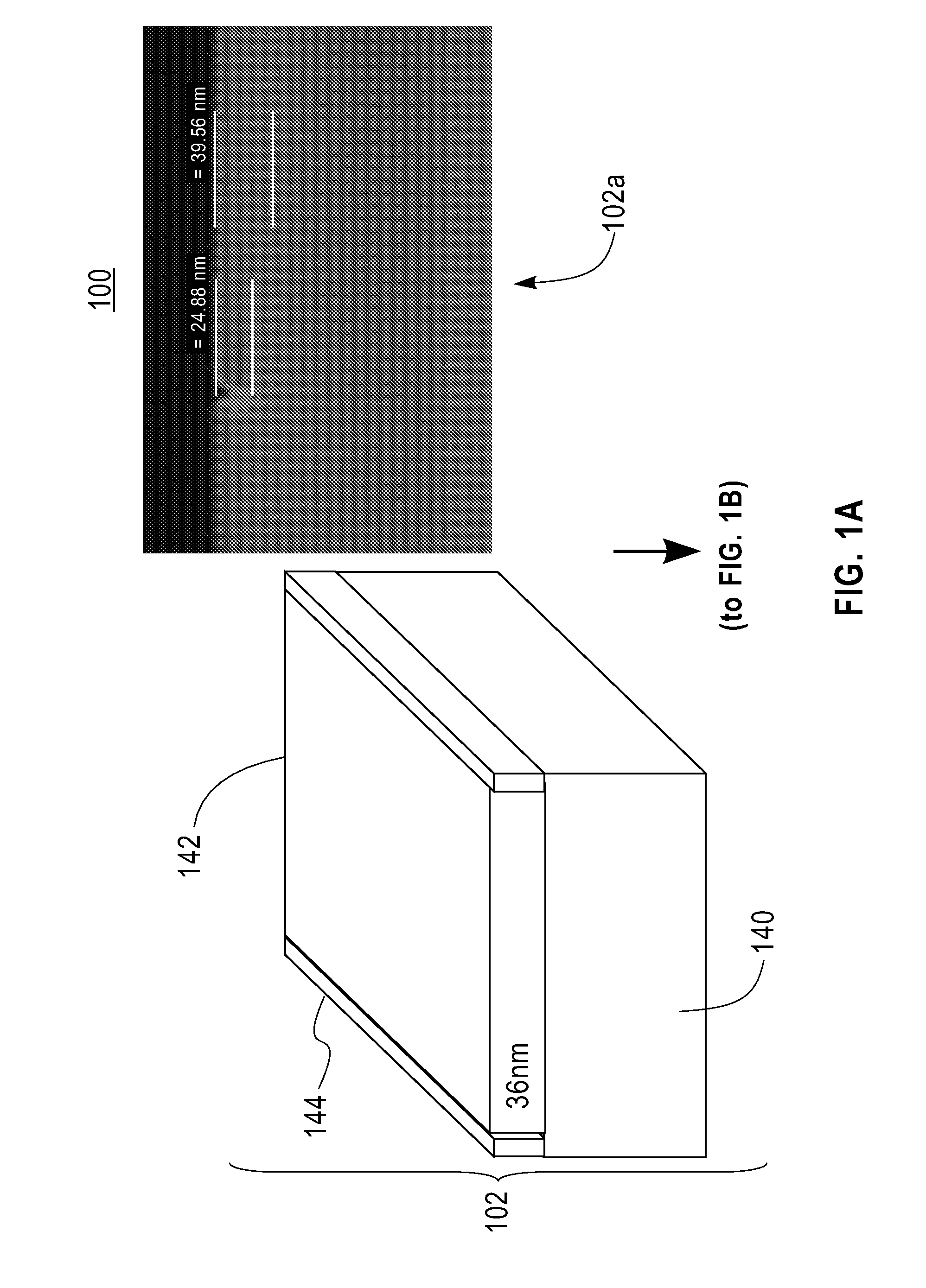
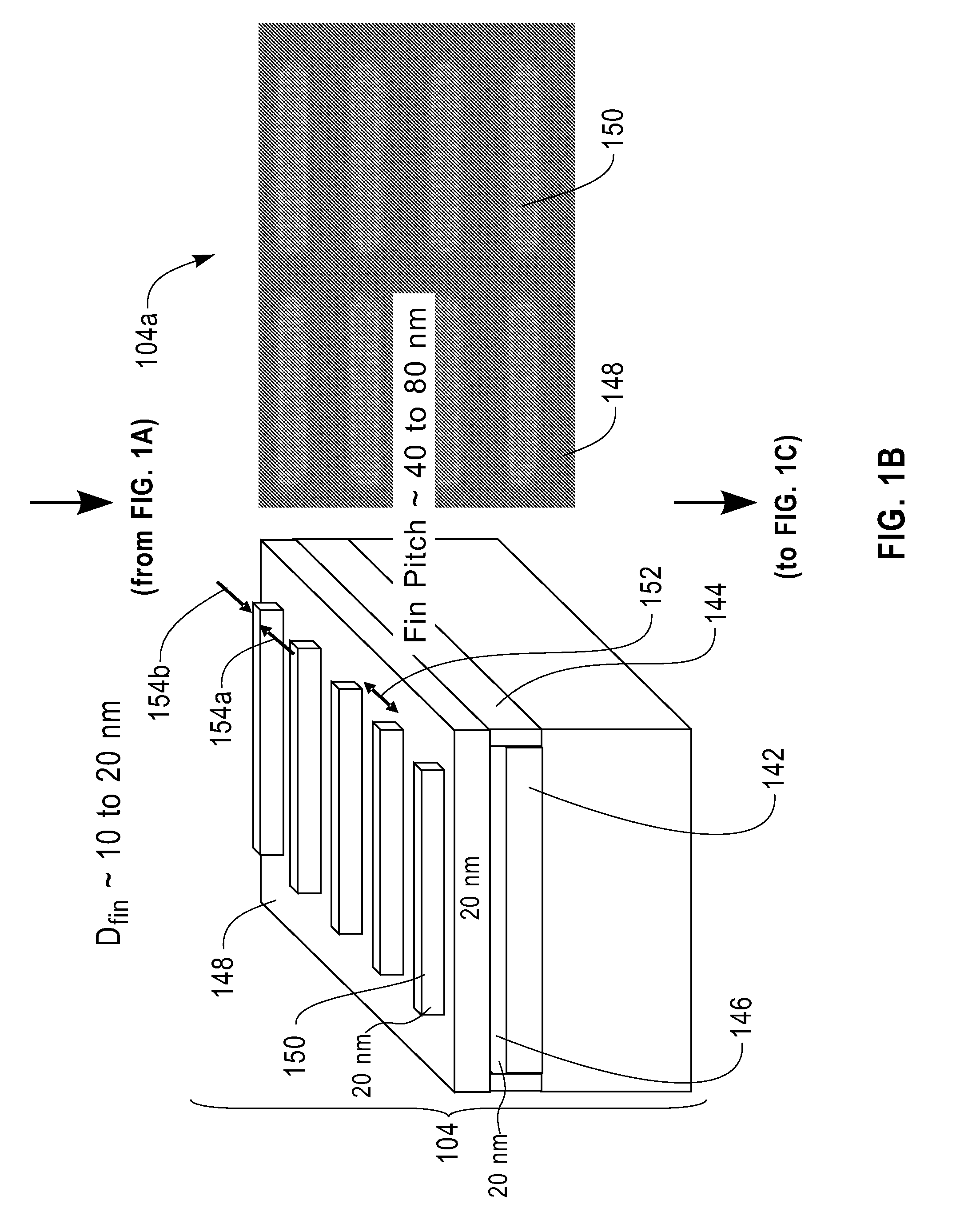
[0029]In step 102, shallow trench isolation (STI) is used to define a silicon active area in a silicon-on-insulator (SOI) substrate. Namely, a substrate, i.e., substrate 140, is provided. The substrate can comprise any suitable insulator material including, but not limited to, dielectric materials, such as silicon dioxide (SiO2). According to an exemplary embodiment, substrate 140 has a nitride layer. i.e., nitride layer 144, thereon. A trench is etched in nitride layer 144 and silicon is deposited in the trench to form silicon layer 142. Excess silicon can be removed from silicon layer 142 using a planarization technique, such as chemical-mechanical planarization (CMP). According to an e...
PUM
 Abstract
Description
Claims
Application Information