

Methods and apparatus for EMI shielding in multi-chip modules
a multi-chip module and electromagnetic shielding technology, applied in the direction of cross-talk/noise/interference reduction, printed circuit aspects, rigid plastic container screening, etc., can solve the problems of increasing the size of the component, and increasing the size of the semiconductor devi
- Summary
- Abstract
- Description
- Claims
- Application Information
AI Technical Summary
Benefits of technology
Problems solved by technology
Method used
Image

Examples
Embodiment Construction
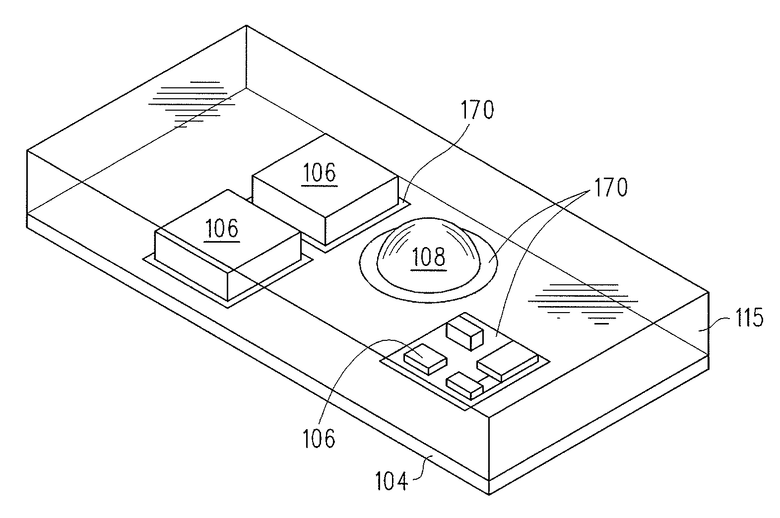
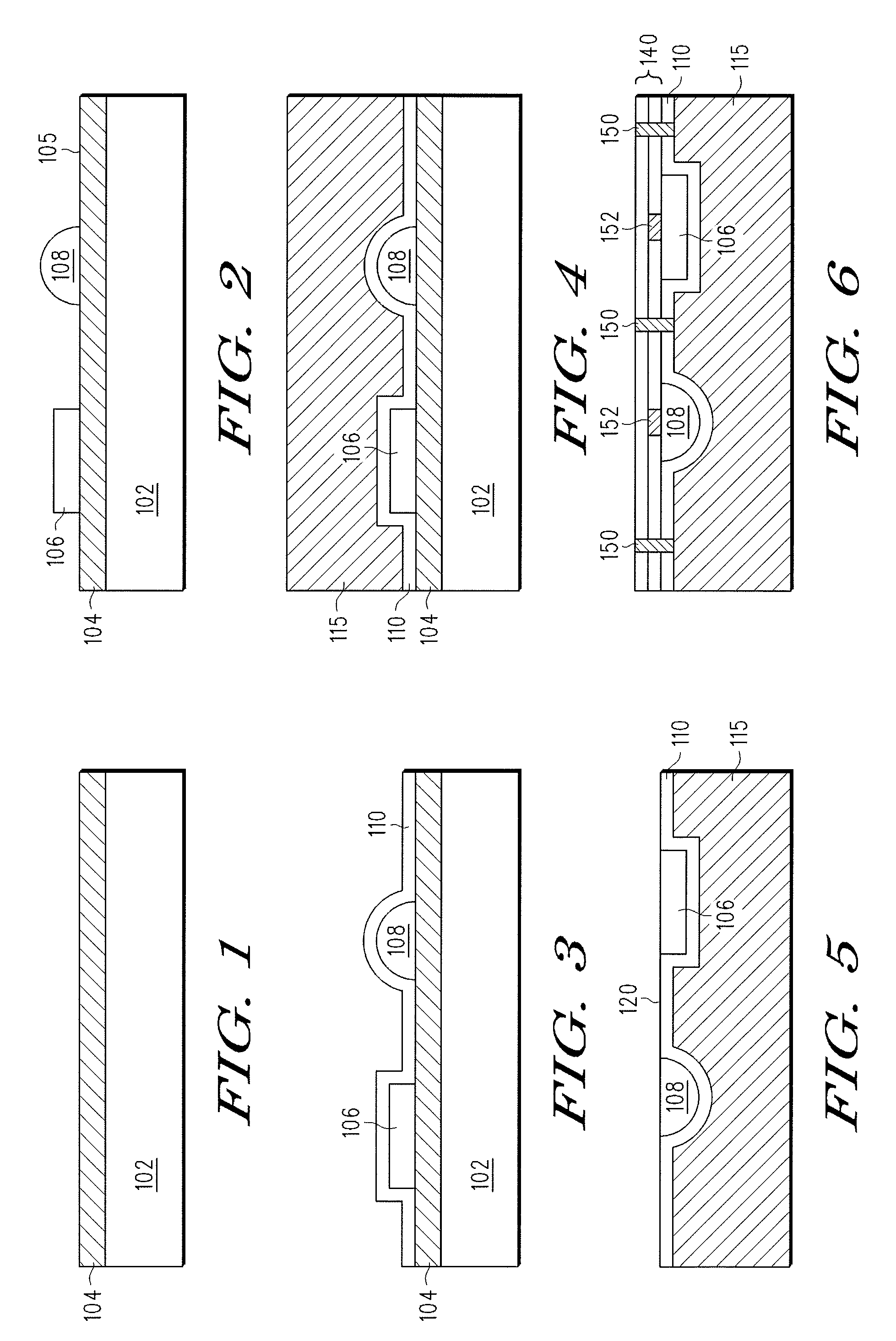
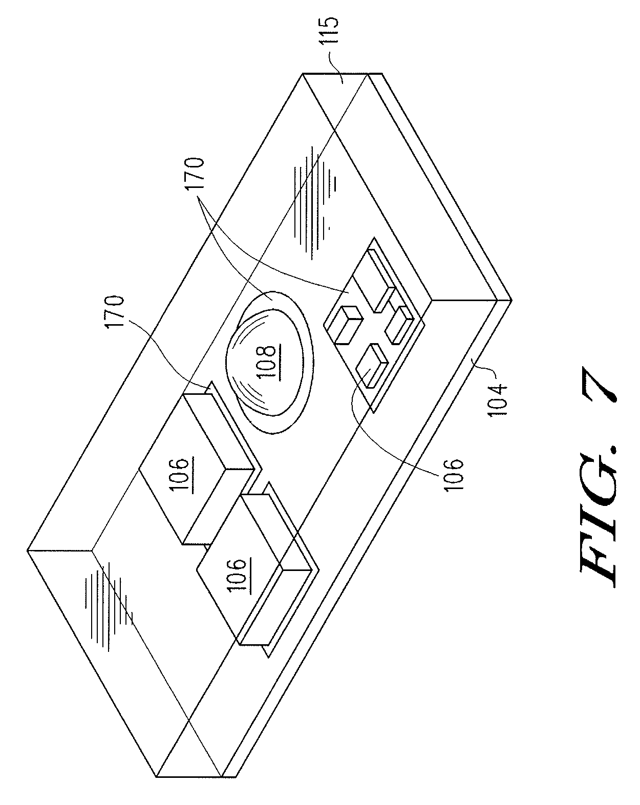
[0009]The following detailed description is merely exemplary in nature and is not intended to limit the invention or the application and uses of the invention. Furthermore, there is no intention to be bound by any expressed or implied theory presented in the preceding technical field, background, or the following detailed description. For the sake of brevity, conventional techniques related to semiconductor processing, electronic packaging, and device assembly are not described herein.
[0010]For simplicity and clarity of illustration, the drawing figures depict the general structure and / or manner of construction of the various embodiments. Descriptions and details of well-known features and techniques may be omitted to avoid unnecessarily obscuring other features. Elements in the drawings figures are not necessarily drawn to scale: the dimensions of some features may be exaggerated relative to other elements to assist improve understanding of the example embodiments.
[0011]Terms of en...
PUM
 Abstract
Description
Claims
Application Information