
Thin-film transistor device and a method for manufacturing the same

a transistors, which is applied in the direction of thermoelectric device junction materials, semiconductor devices, electrical apparatus, etc., can solve the problems of inability to meet the needs of reducing power consumption or realizing sophisticated devices, and the underlying technology of thin-film transistors, so as to reduce the number of steps in manufacturing and reduce the number of steps. , the effect of low power consumption

Inactive Publication Date: 2009-01-01
HITACHI LTD
View PDF8 Cites 18 Cited by
  • Summary
  • Abstract
  • Description
  • Claims
  • Application Information

AI Technical Summary

Benefits of technology

The present invention provides a method for manufacturing a thin-film transistor (TFT) that can be used in flexible and thin-lightweight electronic devices such as displays and RF-ID cards. The method simplifies the manufacturing process and reduces manufacturing costs compared to existing techniques. The TFTs formed using this method have high performance and low power consumption, and can be used in complementary TF circuits. The invention also provides a thin-film transistor device comprising an n-type and p-type TFTs, where the semiconductor film for forming a channel is made of the same material for both TFTs, and the source and drain electrodes are made of the same material. This simplifies the manufacturing process and reduces power consumption. The invention also reduces the number of steps in manufacture and facilitates mass production.

Problems solved by technology

A technique on a transistor substrate required for realization of devices capable of satisfying the needs as described above is associated with an organic thin-film transistor belonging to the first example of the related art described above; however, the organic thin-film transistor is based on a single channel, and cannot be used for configuring a complementary circuit.
Therefore this technique cannot satisfy the needs for reduction in power consumption or for realization of sophisticated devices.
In the case of the complementary TFT circuit belonging to the second example of the related art described above, because different semiconductor materials are used for the n-type TFT and the p-type TFT, film formation and machining for the materials, and patterning are required to be carried out separately according to each material, and the production process is complicated.
As a result, it is difficult to simplify the production process and to reduce the manufacturing cost with this technique.

Method used


Image

  • Thin-film transistor device and a method for manufacturing the same
  • Thin-film transistor device and a method for manufacturing the same
  • Thin-film transistor device and a method for manufacturing the same

Examples


first embodiment

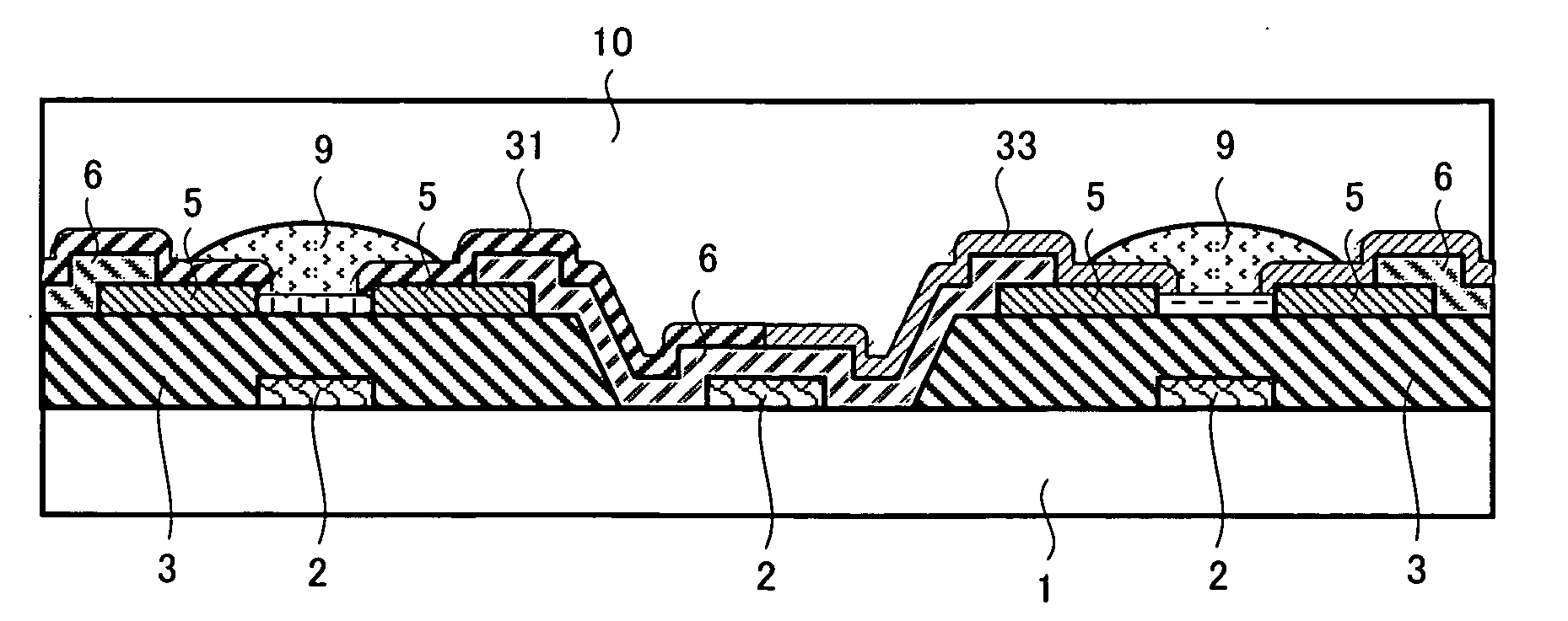
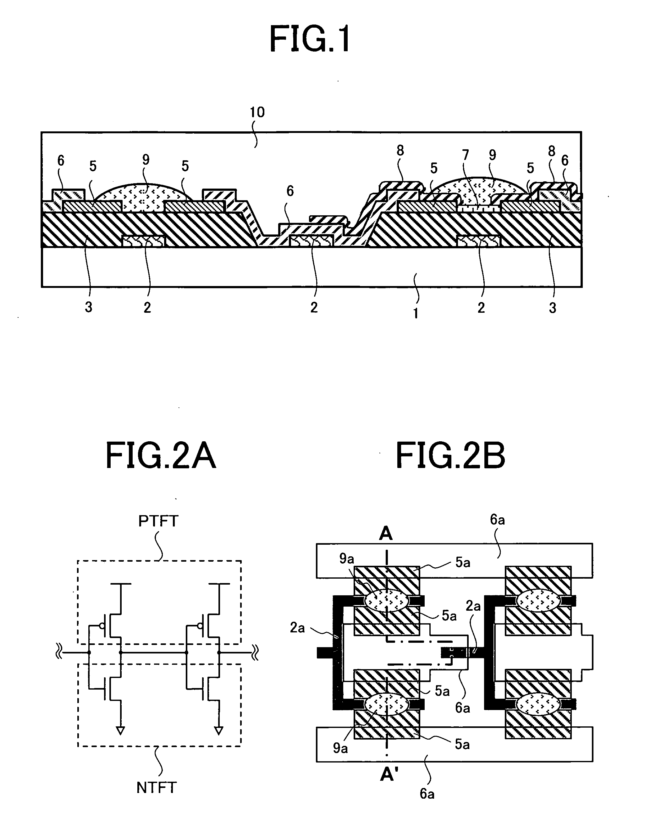
[0049]A first embodiment of the present invention is described with reference to FIGS. 1 to 10. This embodiment relates to an example of a thin film transistor formed by the solution-process and / or printable process method, for instance, on a flexible substrate in which a complementary TFT circuit is configured with a p-type TFT and an n-type TFT. The examples of circuits provided in this embodiment are a signal generator including a ring oscillator and a NAND circuit. The complementary TFT circuit as represented by the circuits operates with low power consumption, and can provide various functions or systems.

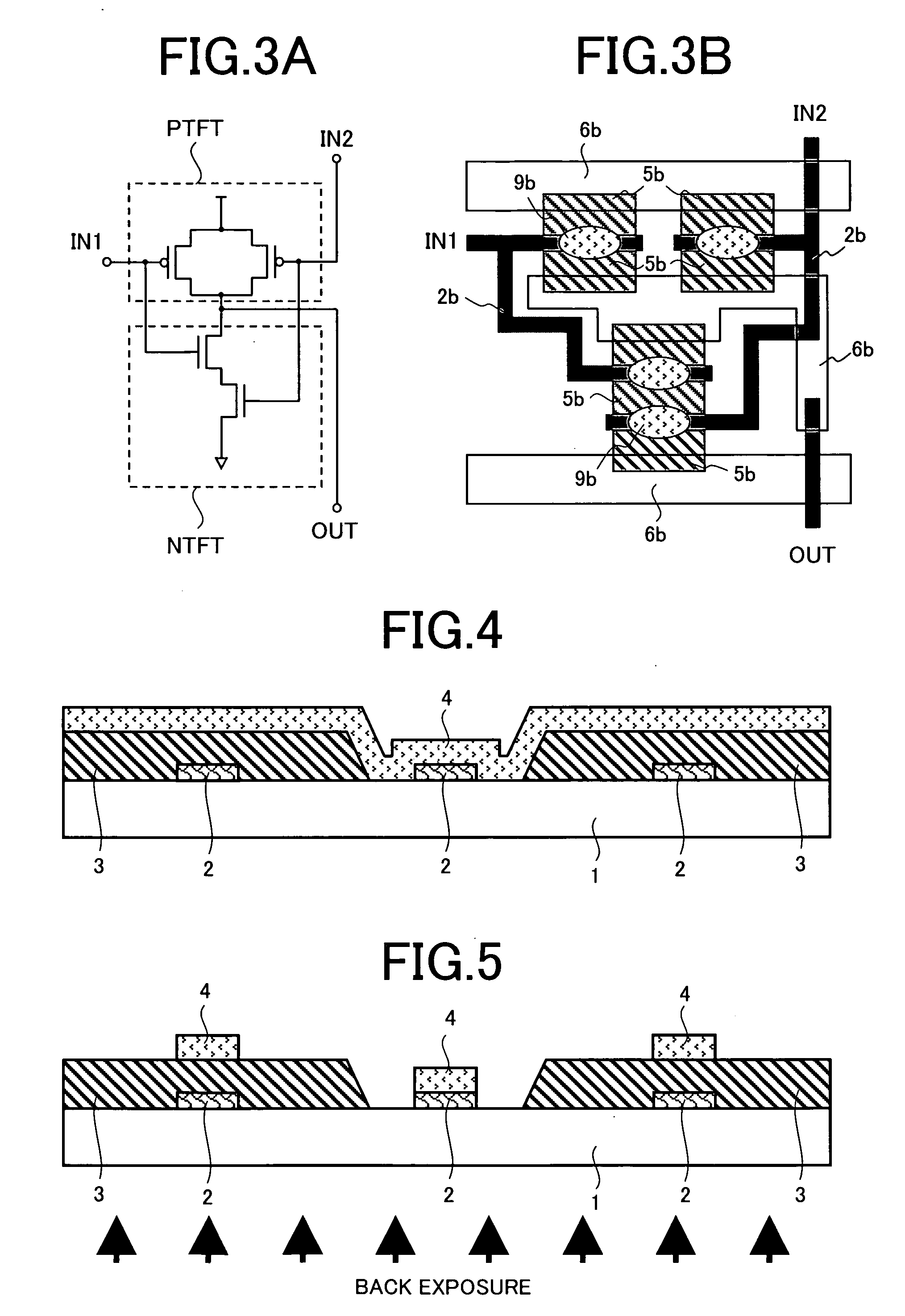
[0050]The ring oscillator has a plurality of complementary TFT invertors connected in multiple stages. FIG. 2A is a circuit diagram showing two stages of the invertors, and FIG. 2B is a plan view showing the layout. The NAND circuit shown in FIG. 3 is one of basic logic circuits required to constitute an electronic computer. FIG. 3A is a circuit diagram illustrating a two-input...

second embodiment

[0078]A second embodiment of the present invention is described with reference to FIGS. 11 to 13, and FIG. 7. The second embodiment exemplifies a tin-film transistor device on which the same complementary TFT circuit as that in the first embodiment is configured. In the second embodiment, the manufacturing steps 1 to 3 in the first embodiment shown in FIGS. 4 to 6 are replaced with those shown in FIGS. 11 to 13, and other manufacturing steps or the cross-sectional structure of the completed device as shown in FIG. 1 are the same as those in the first embodiment.

[0079]Outlines of the replaced steps are as described below.

[0080]Specifically, as shown in FIG. 11, the steps of forming the gate electrode 2 on the transparent plastic substrate 1 using a metal ink material by the print-patterning method and applying the Si oxide film 3 to provide an opening for connection are the same as the steps 1 in the first embodiment.

[0081]Then, a photo-sensitive SAM film, from which the hydrophobic ...

third embodiment

[0088]A third embodiment of the present invention is described with reference to chemical formulae 1 to 9 shown in FIG. 19 and chemical formulae 10 to 12 shown in FIG. 20. In this embodiment, example of materials for the polarizable thin films 7, 8 used in the first embodiment are shown with the chemical formulae.

[0089]Chemical formulae 1 to 7 represent examples of polarizable SAM material generating a dipole vector from the gate insulator 3 (for instance, Si oxide film) or the source / drain electrodes 5 to the organic semiconductor in the n-type TFT. In the chemical formulae, X denotes an SH group or a silane coupling group expressed by chemical formula 12. R1, R2, and R3 in chemical formula 12 denote an OCH3 group, an OCH2CH3 group or an OH group, or CL (chlorine). The polarizable thin film material adheres to electrodes when X is an SH group, and generates a dipole vector from the source / drain electrode to the organic semiconductor 9. When X is a silane coupling group, the thin fi...


PUM


Abstract

The present invention provides a method of manufacturing a thin-film transistor device. This method enables improvement in performance of a complementary TFT circuit incorporated in a thin- and light-weighted image display device or a flexible electronic device and also enables reduction of power consumption and reduction of manufacturing cost of the circuit. Further in the method, the number of manufacturing steps is decreased so that mass production and growth in size of thin film transistor devices are facilitated through a printing technique. In this method, electrodes forming n-type and p-type TFT and an organic semiconductor are made of the same material in both types of TFT by the solution-process and / or printable process method. A first polarizable thin-film 7 is formed on an interface between a gate insulator and a semiconductor, and also a second polarizable thin film 8 provided on an interface between source and drain electrodes 5 and a semiconductor film 9. A complementary thin-film transistor device is manufactured by selectively exposing either the n-type TFT area or the p-type TFT area to light to remove the polarizing function from the first and second polarizable thin films in the area.

Description

CLAIM OF PRIORITY[0001]The present application claims priority from Japanese patent application JP 2007-160621 filed on Jun. 18, 2007, the content of which is hereby incorporated by reference into this application.BACKGROUND OF THE INVENTION[0002]1. Field of the Invention[0003]The present invention relates to a method of manufacturing a thin-film transistor device and a thin-film transistor device. More specifically, the invention relates to a thin-film transistor device and a method of manufacturing a thin-film transistor device which enables reduction in manufacturing cost and is excellent in thin and light-weight characteristics, impact resistance as well as flexibility. This method advantageously is suitable for a transistor integrated circuit substrate or an active matrix image display device.[0004]2. Description of the Related Art[0005]As a first example of the related art, a thin-film transistor (referred to as TFT hereinafter) which uses an organic semiconductor and an activ...

Claims


Application Information

Patent Timeline
Patent Type & Authority Applications(United States)
IPC IPC(8): H01L51/00H01L51/40H10K99/00
CPCH01L27/283H01L51/0004H01L51/0012H01L51/105H01L51/0545H01L51/0558H01L51/0022H10K19/10H10K71/13H10K71/191H10K71/611H10K10/484H10K10/84H10K10/466
Inventor SHIBA, TAKEOHASHIZUME, TOMIHIROSUWA, YUJIARAI, TADASHI
Owner HITACHI LTD
Learn More