

Transparent Conductive Laminate and Transparent Touch Panel Comprising the Same
a technology of transparent conductive laminate and touch panel, which is applied in the direction of conductive layers on insulating supports, instruments, insulating bodies, etc., can solve the problems of deteriorating display visibility, color separation (sparkling) of light from the display, and deteriorating display visibility, so as to prevent the deterioration of display visibility, excellent transparency, and small haze value
- Summary
- Abstract
- Description
- Claims
- Application Information
AI Technical Summary
Benefits of technology
Problems solved by technology
Method used
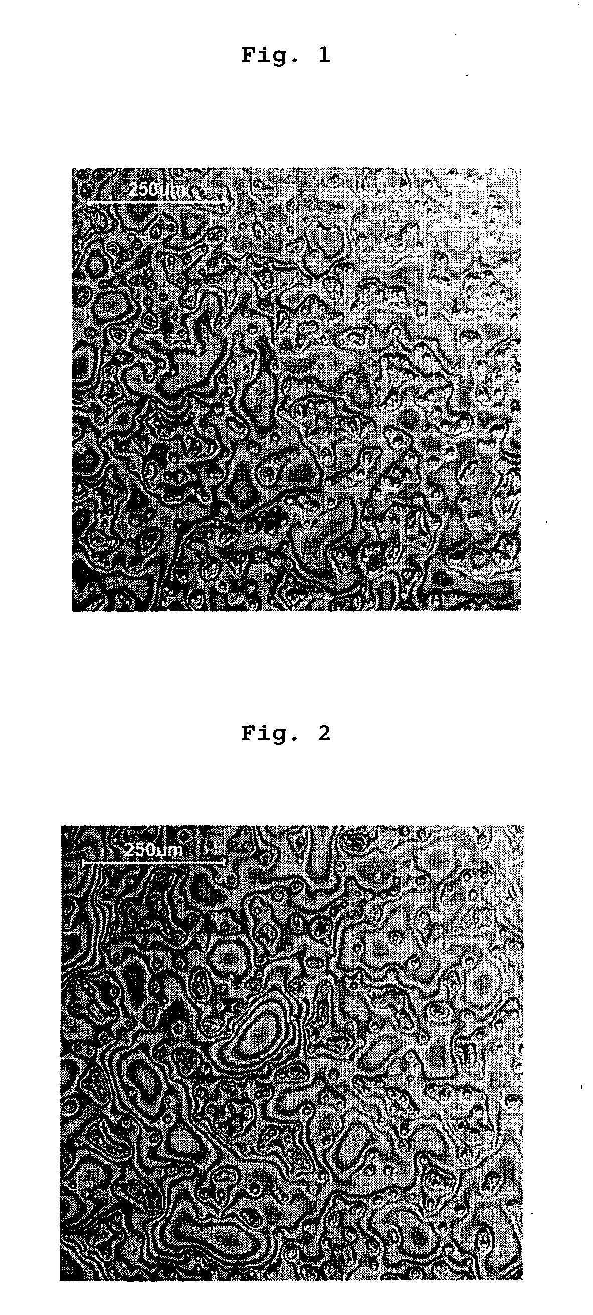
Image

Examples
example 1
[0091]100 parts by weight of the Aronix M405 tetrafunctional acrylate (of Toagosei Chemical Industry Co., Ltd.), 5 parts by weight of Irgacure 184 (of Chiba Specialty Chemicals Co., Ltd.) and 0.7 part by weight of Hipresica (3.0 μm product, grade of N3N) of Ube-Nitto Kasei Co., Ltd. were dissolved in a 1:1 mixed solvent of isopropyl alcohol and 1-methoxy-2-propanol to prepare a coating solution A. The coating solution A and MgF2 fine particles having an average primary particle diameter of 30 nm (of CI Kasei Co., Ltd., dispersion containing 20 wt % of a mixed solvent of ethyl alcohol and n-butyl alcohol) were mixed with 100 parts by weight of a curable resin component to prepare a coating solution B having a solid content of 5 parts by weight.
[0092]The coating solution B was applied to one side of a polyethylene terephthalate film (OFW-188 of Teijin Du Pont Film Co., Ltd.) on a transparent polymer substrate to a thickness of 2.5 μm after curing with a bar coater, dried at 50° C. for...
example 2
[0097]A transparent conductive laminate and a transparent touch panel were manufactured in the same manner as in Example 1 except that 0.2 part by weight of the Hypresica of Ube Nitto Kasei Co., Ltd. (2.0 μm product, grade of N3N) was added to the coating solution A of Example 1. The measurement results of the haze value, Ra and Rz of the transparent conductive laminate and the evaluation results of the anti-sparkling and anti-Newton rings properties of the transparent touch panel are shown in Table 1.
example 3
[0098]A transparent conductive laminate and a transparent touch panel were manufactured in the same manner as in Example 1 except that the transparent polymer substrate of Example 1 was changed to the Zeonoa (ZF14-100) of Nippon Zeon Co., Ltd. The measurement results of the haze value, Ra and Rz of the transparent conductive laminate and the evaluation results of the anti-sparkling and anti-Newton rings properties of the transparent touch panel are shown in Table 1.
PUM
| Property | Measurement | Unit |
|---|---|---|
| Fraction | aaaaa | aaaaa |
| Percent by mass | aaaaa | aaaaa |
| Length | aaaaa | aaaaa |
Abstract
Description
Claims
Application Information