
Method for driving ccd-type solid-state imaging device and imaging apparatus

Inactive Publication Date: 2009-01-01
FUJIFILM CORP
View PDF6 Cites 2 Cited by
  • Summary
  • Abstract
  • Description
  • Claims
  • Application Information

AI Technical Summary

Benefits of technology

[0010]The invention provides a method for driving a CCD-type solid-state imaging device and an imaging apparatus, which can take a high quality photographic image over a whole screen without narrowing a dynamic range of an image.
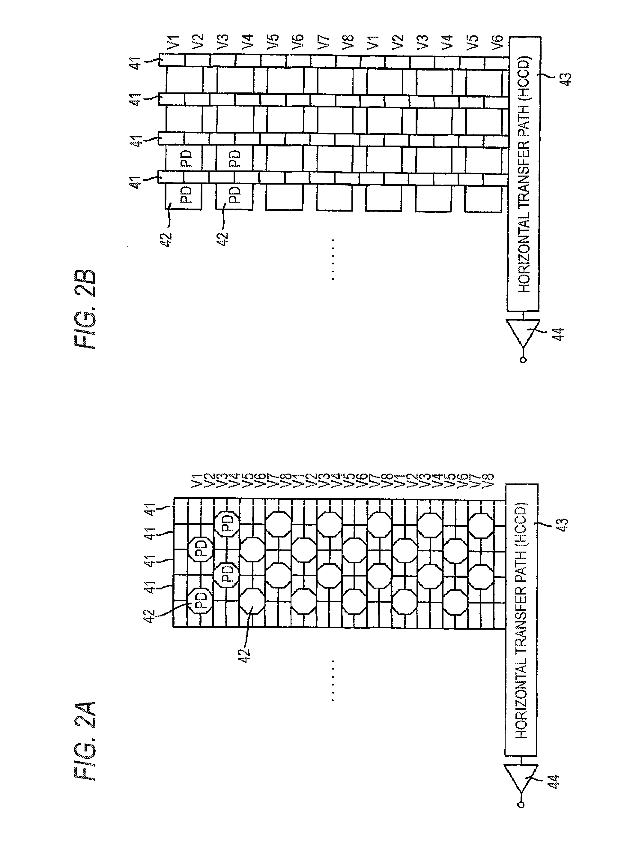
[0011]According to one aspect of the invention, a method for driving a CCD-type solid-state imaging device includes: reading charges detected by photoelectric conversion elements into potential packets formed in a charge transfer path; dividing each potential packet into plural segment packets while narrowing a range where the charges are present in each potential packet, by moving a split barrier from one side of each potential packet toward the other side of each potential packet, wherein each split barrier has a lower potential height than a partition barrier that forms a boundary between the adjacent potential packets; and transferring the charges along the charge transfer path after the dividing.
[0023]With the above configuration, the capacity of the potential packets is decreased during transfer. Hence, it is possible to decrease a dark current mixed into signal charges. In addition, even when an empty packet is generated among segment potential packets, signals of the empty packet are not added. Therefore, it is possible to decrease a dark current in a low luminance portion (dark portion) in an taken image of one screen and thus to obtain a high quality image.

Problems solved by technology

As a result, it may be difficult to obtain a high quality image over the whole screen.
However, by doing so, it is necessary to decrease a saturation signal charge amount of the high luminance image, which may narrow a dynamic range of an image.

Method used


Image

  • Method for driving ccd-type solid-state imaging device and imaging apparatus
  • Method for driving ccd-type solid-state imaging device and imaging apparatus
  • Method for driving ccd-type solid-state imaging device and imaging apparatus

Examples


Embodiment Construction

[0031]Now, embodiments of the invention will be described with reference to the drawings.

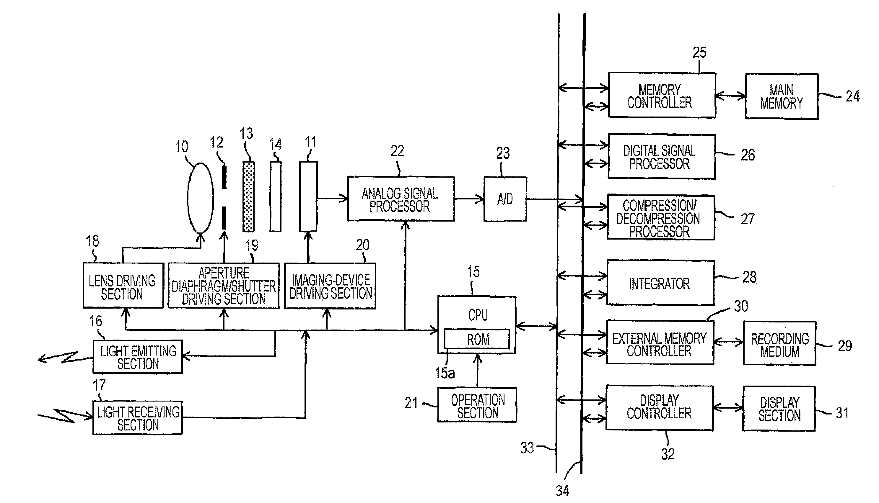
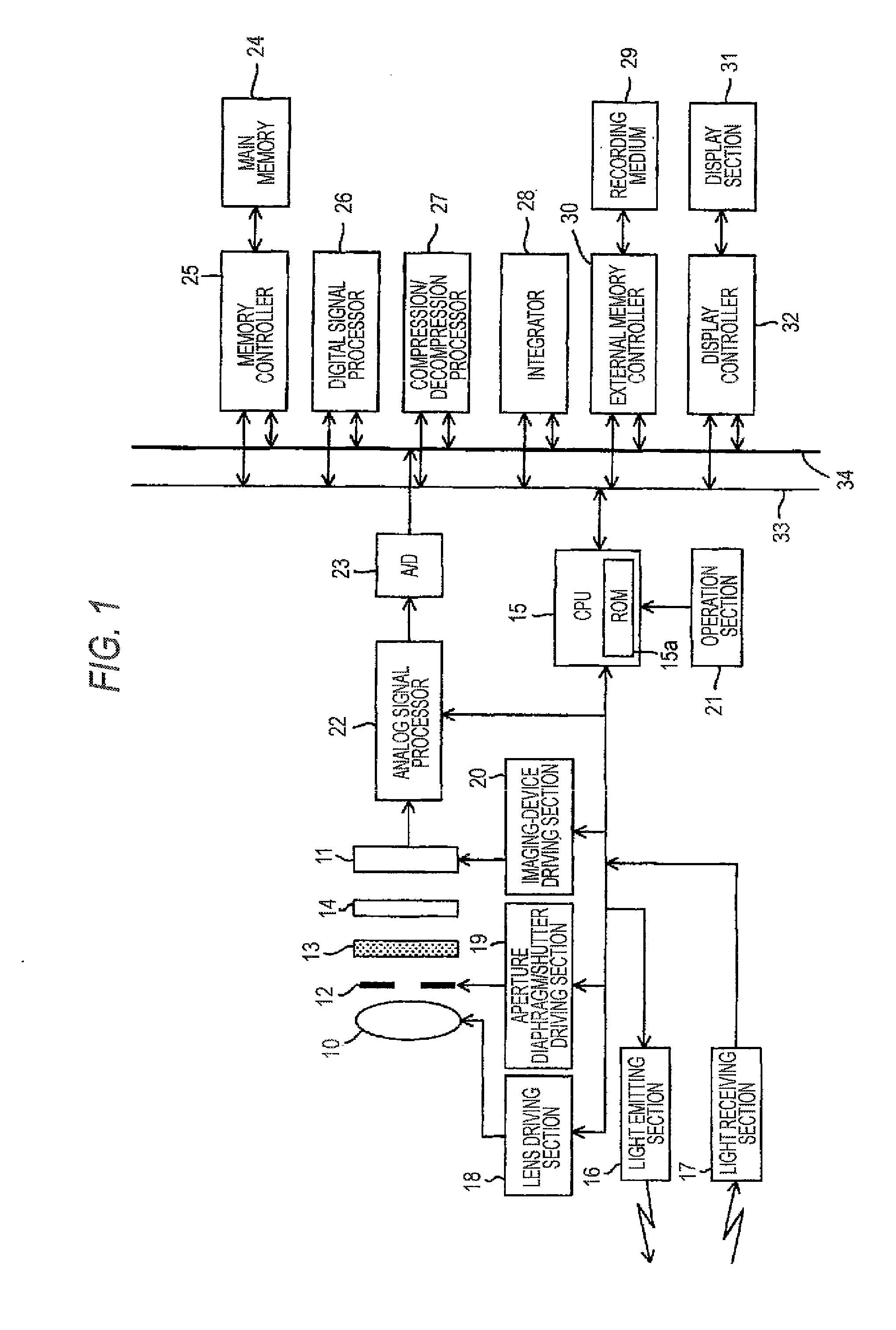
[0032]FIG. 1 is a diagram showing the configuration of a digital still camera according to a first embodiment of the invention. This embodiment will be described by way of an example of a digital still camera. However, the invention can be applied to a digital video camera or other digital cameras, for example, one mounted on a small electronic device such as a mobile phone.

[0033]The digital still camera shown in FIG. 1 includes an imaging lens 10, a CCD-type solid-state imaging device 11, and an aperture diaphragm and a mechanical shutter 12 that are disposed between the imaging lens 10 and the solid-state imaging device 11, an infrared cut filter 13, and an optical low-pass filter 14. A CPU 15 controls the overall operation of the digital still camera. The CPU 15 also controls a flash light emitting section 16 and a light receiving section 17. The CPU 15 also controls a lens driving section 18...


PUM


Abstract

A method for driving a CCD-type solid-state imaging device includes: reading charges detected by photoelectric conversion elements into potential packets A (B) formed in a charge transfer path, dividing each potential packet A (B) into plural segment packets A1, A2 (B1, B2) while narrowing a range where the charges are present in each potential packet A (B), by moving a split barrier D from one side of each potential packet A (B) toward the other side of each potential packet A (B), and transferring the charges along the charge transfer path after the dividing. Each split barrier D has a lower potential height than a partition barrier C that forms a boundary between the adjacent potential packets A, B.

Description

CROSS-REFERENCE TO RELATED APPLICATIONS[0001]This application is based upon and claims the benefit of priority from the Japanese Patent Application No. 2007-133100 filed on May 18, 2007, the entire contents of which are incorporated herein by reference.BACKGROUND OF THE INVENTION[0002]1. Technical Field[0003]The invention relates to a method for driving a CCD (Charge Coupled Device) type solid-state imaging device and an imaging apparatus, and more particularly, to a method for driving a CCD-type solid-state imaging device and an imaging apparatus, which are suitable to reduce a dark current component contained in a low luminance image portion of a taken image.[0004]2. Description of the Related Art[0005]CCD-type solid-state imaging devices are configured to transfer signal charges detected by photoelectric conversion elements via charge transfer paths, for output. Therefore, a dark current may be mixed into the signal charges during the charge transfer. The influence of the dark cu...

Claims


Application Information

Patent Timeline
IPC IPC(8): H04N5/335H01L27/148H04N5/341H04N5/355H04N5/361H04N5/369H04N5/372H04N5/378H04N101/00
CPCH01L27/14831H04N2101/00H04N5/3728H04N5/361H04N25/63H04N25/73
Inventor KOBAYASHI, HIROKAZU
Owner FUJIFILM CORP
Learn More