Semiconductor device and method of fabricating the same

Active Publication Date: 2005-03-22
FUJITSU SEMICON LTD
View PDF6 Cites 4 Cited by
  • Summary
  • Abstract
  • Description
  • Claims
  • Application Information

AI Technical Summary

Benefits of technology

An object of the present invention is to provide a semiconductor device which avoids a decrease in the current-driving capacity of a transistor operating at a low voltage while ensuring the reliability of a ga

Problems solved by technology

However, the present inventors consider that the above-described conventional method of fabricating semiconductor devices has the following problems.
For this reason, a parasitic transistor occurs parallel to the memory cell, with the result that humps occur in the current-voltage characteristics of the memory cell, causing an increase in leakage current.
In this case, however, the area of the element region inevitably becomes small, with the result that the current-driving capacity of the transistor constituting the peripheral circuit decreases, causing a decrease in the operating speed.
When the curvature of the interface between the top e

Method used


Image

  • Semiconductor device and method of fabricating the same
  • Semiconductor device and method of fabricating the same
  • Semiconductor device and method of fabricating the same

Examples


Example

First Embodiment

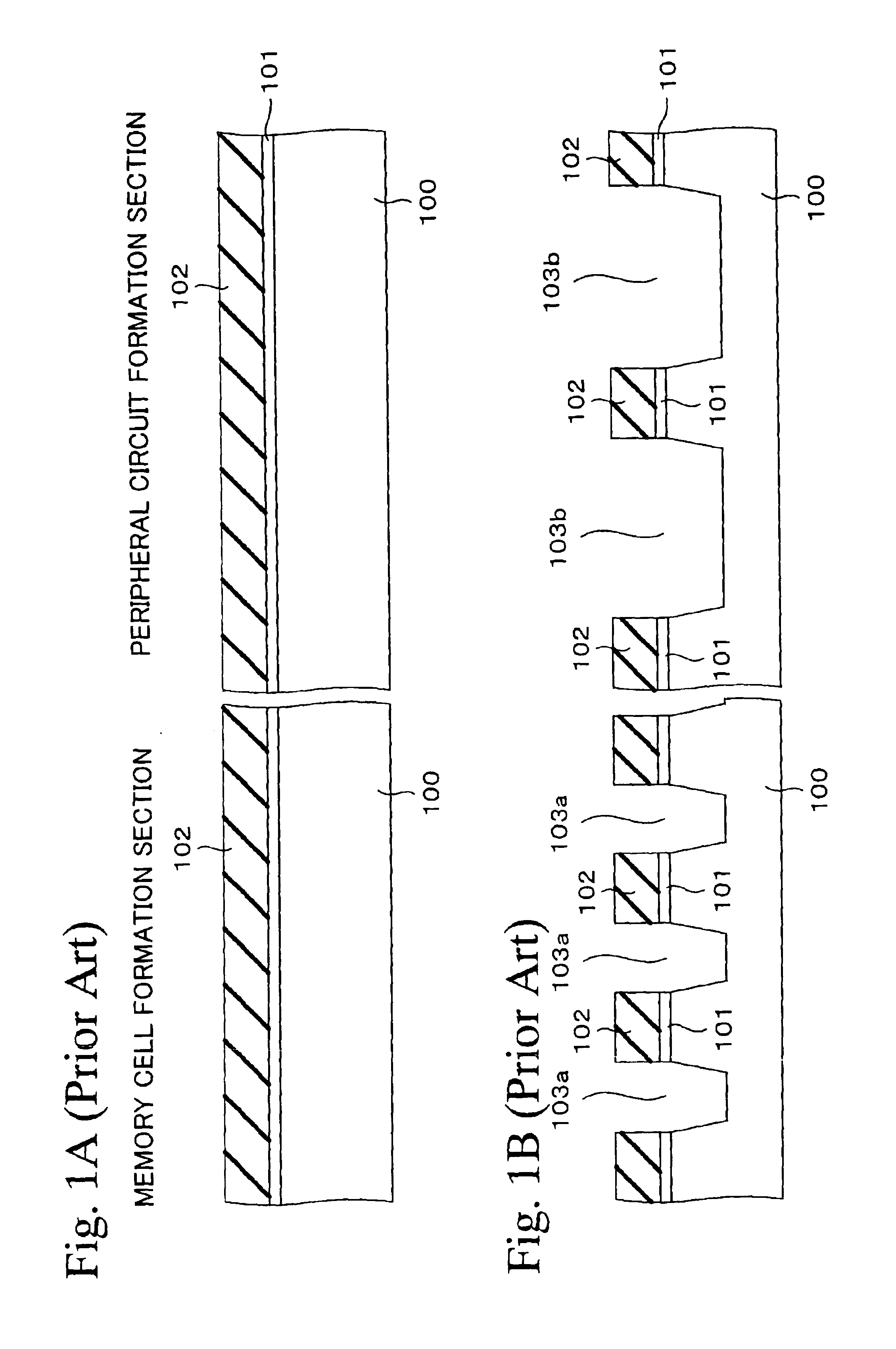
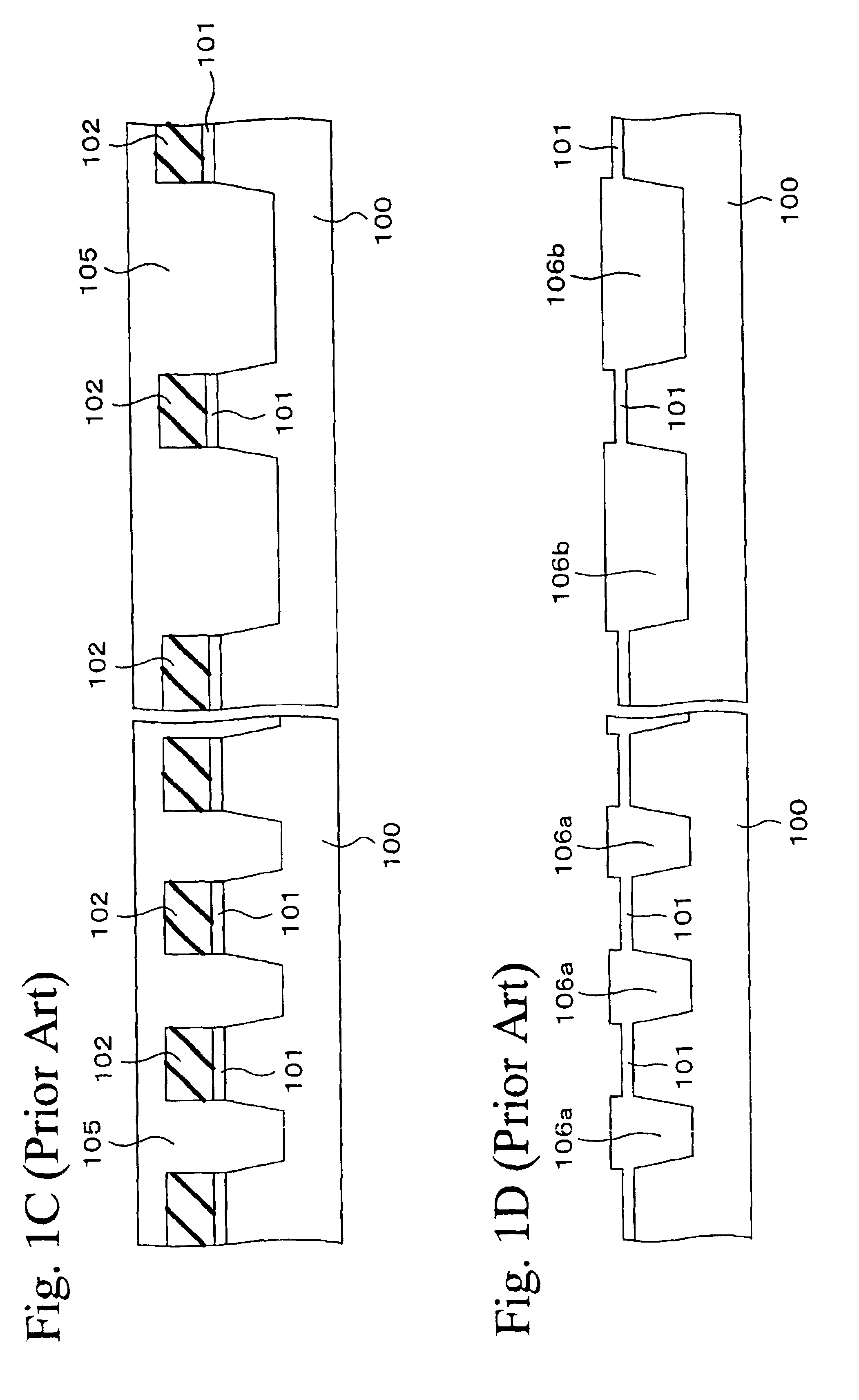
FIGS. 3A to 3I are sectional views showing a fabrication method of a semiconductor device in a first embodiment of the present invention in the order of steps. Incidentally, this embodiment shows an example in which the invention is applied to the fabrication of a flash memory (EEPROM) having a memory cell and a peripheral circuit to drive the memory cell. In FIGS. 3A to 3I, the cross section of a memory-cell formation section is shown in the left-hand part of each view and the cross section of a peripheral-circuit formation section is shown in the right-hand part.

First, as shown in FIG. 3A, a pad oxide film 11 is formed on a semiconductor substrate 10 by the thermal oxidation process, for example, and a silicon nitride film 12 is formed on the pad oxide 11 film by the CVD process. Incidentally, a film of laminated structure of a silicon oxide layer and a silicon nitride layer may be formed in place of the silicon nitride film 12.

Next, as shown in FIG. 3B, by etching...

Example

Second Embodiment

FIGS. 5A to 5I are sectional views showing a fabrication method of a semiconductor device (a flash memory) in a second embodiment of the present invention in the order of steps. In these FIGS. 5A to 5I, the section of a memory-cell formation section is shown in the left-hand part of each view and the section of a peripheral-circuit formation section is shown in the right-hand part.

First, as shown in FIG. 5A, a pad oxide film 21 is formed on a semiconductor substrate 10 by, for example, the thermal oxidation process. And the memory-cell formation section is covered with a resist film (not shown) and, as shown in FIG. 5B, the pad oxide film 21 of the peripheral-circuit formation section is removed.

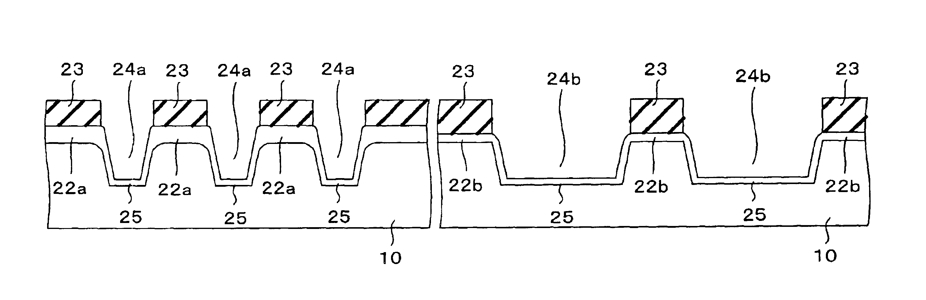
Next, as shown in FIG. 5C, by performing again the thermal oxidation of the surface of the semiconductor substrate 10, a pad oxide film 22a is formed in the memory-cell formation section and a pad oxide film 22b is formed in the peripheral-circuit formation section.

Next, as ...

Example

Third Embodiment

FIGS. 6A to 6G are sectional views showing a fabrication method of a semiconductor device (a flash memory) in a third embodiment of the present invention in the order of steps. In these FIGS. 6A to 6G, the section of a memory-cell formation section is shown in the left-hand part of each view and the section of a peripheral-circuit formation section is shown in the right-hand part.

First, as shown in FIG. 6A, a pad oxide film 31 is formed on a semiconductor substrate 10 by, for example, the thermal oxidation process, and a silicon nitride film 32 is formed on the pad oxide film 31 by the CVD process. A film of laminated structure of a silicon oxide layer and a silicon nitride layer may be formed in place of the silicon nitride film 32.

Next, as shown in FIG. 6B, a resist film 33 having an opening in a part corresponding to the element-isolating region of the memory-cell formation section is formed on a silicon nitride film 32. And after the sequential etching of the sil...


PUM


Abstract

A pad oxide film and a silicon nitride film are formed on a semiconductor substrate. Next, after the patterning of the silicon nitride film, by etching the pad oxide film and the substrate, a first trench is formed in a first region and a second trench is formed in a second region. After that, by performing side etching of the pad oxide film of the first region while protecting the second region with a resist, a gap is formed between the substrate and the silicon nitride film. Subsequently, the inner surfaces of the first and second trenches are oxidized. At this time, a relatively large volume of oxidizing agent (oxygen) is supplied to a top edge portion of the first trench, and the curvature of the corner of the substrate increases.

Description

CROSS-REFERENCE TO RELATED APPLICATIONSThis application is based upon and claims priority of Japanese Patent Application No. 2002-255471, filed on Aug. 30, 2002, the contents being incorporated herein by reference.BACKGROUND OF THE INVENTION1. Field of the InventionThe present invention relates to a semiconductor device in which element regions are isolated by trenches formed in a semiconductor substrate and a method of fabricating this semiconductor device. More particularly, the invention relates to a semiconductor device in which a transistor operating at a high voltage and a transistor operating at a low voltage are formed on the same semiconductor substrate and a method of fabricating this semiconductor device.2. Description of the Prior ArtIn recent years, collective erasing type flash memories such as EEPROMs (electrically erasable programmable read only memories) have begun to be used in IC cards etc. A memory cell of an EEPROM has two gate electrodes of a floating gate and ...

Claims


Application Information

Patent Timeline
IPC IPC(8): H01L21/70H01L21/76H01L27/115H01L29/66H01L29/78H01L27/108H01L21/8239H01L21/82H01L21/8247H01L27/105H01L29/788H01L29/792H01L27/08H01L27/10H01L21/762H01L31/062
CPCH01L21/76229H01L27/105H01L27/11546H01L27/11543H01L27/11526H10B41/40H10B41/48H10B41/49H01L21/762
Inventor SAITO, HITOSHI
Owner FUJITSU SEMICON LTD
Why Eureka
Try Eureka