

Wireless IC device
a technology of integrated circuits and wires, applied in the direction of instruments, packaging, transportation and packaging, etc., can solve the problems of increasing the manufacturing cost of packages, increasing the length of manufacturing processes and adding elements, and the inability to attach ic tags to small items, so as to reduce the cost of manufacturing packages and reduce thickness
- Summary
- Abstract
- Description
- Claims
- Application Information
AI Technical Summary
Benefits of technology
Problems solved by technology
Method used
Image

Examples
first preferred embodiment
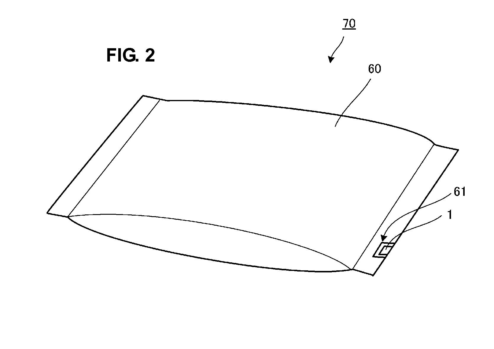
[0058]FIG. 2 is an external perspective view of an article and a wireless IC device attached thereon according to a first preferred embodiment of the present invention. An article 70 can be, for example, a bag of snack food, such as potato chips. An article package 60 preferably is a package in which an aluminum-evaporated laminated film is formed into a bag.
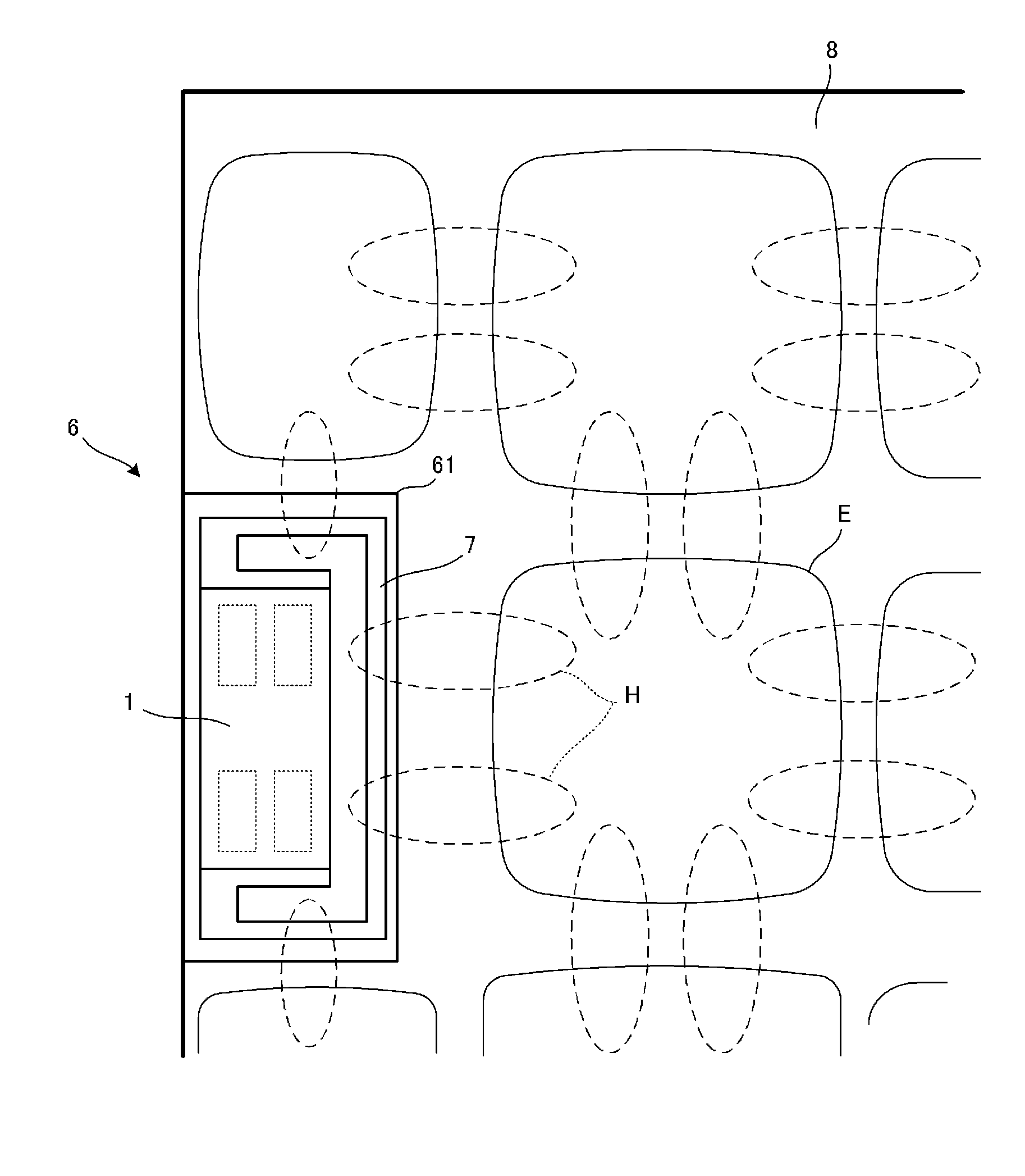
[0059]The article package 60 has a cut-out section (a portion that is not covered with an aluminum-evaporation film) 61 preferably located at an edge. An electromagnetic-coupling module 1 is disposed in the cut-out section 61.
[0060]FIGS. 3A and 3B illustrate a structure of a wireless IC device, showing only component parts of the article 70 illustrated in FIG. 2. In FIGS. 3A and 3B, a radiation electrode 8 corresponds to an aluminum-evaporated layer of the aluminum-evaporated laminated film of the article package 60. A loop electrode 7 is disposed within the cut-out section (a portion where the electrode is not formed) 61 of the...
second preferred embodiment
[0066]FIG. 4 is an external perspective view of an article and a wireless IC device attached thereon according to a second preferred embodiment. An article 71 can be, for example, a bag of snack food. An article package 60 preferably is a package in which an aluminum-evaporated laminated film is formed into a bag.
[0067]In an example illustrated in FIG. 2, the electromagnetic-coupling module is arranged in an edge of the article package. In an example illustrated in FIG. 4, an electromagnetic-coupling module 1 is disposed inside the article package 60 and away from the edge of the article package 60. The article package 60 is formed from an aluminum-evaporated laminated film having a non-conductive section 62 as part thereof. The non-conductive section 62 is not covered with an aluminum-evaporated film. The electromagnetic-coupling module 1 is arranged within the non-conductive section 62 and positioned adjacent to an edge thereof.
[0068]FIG. 5 illustrates a structure of an implementa...
third preferred embodiment
[0071]FIG. 6B illustrates a structure of a main portion of a wireless IC device according to a third preferred embodiment. FIG. 6A is an external view of an article on which the wireless IC device is attached. In FIG. 6A, an article 72 includes a substantially planar metallic body 63 and a wireless-IC-device main portion 6 attached thereon. The substantially planar metallic body 63 is a plate-shaped or sheet-shaped article having a metallic layer contained therein or a metallic plate itself.
[0072]The wireless-IC-device main portion 6 is shaped like a tab index, as illustrated in FIG. 6B, and includes an insulating sheet 64. The insulating sheet 64 includes an adhesive layer on the inside surface and sandwiches a loop electrode 7 and an electromagnetic-coupling module 1. The structure of the loop electrode 7 and that of the electromagnetic-coupling module 1 are substantially the same as those illustrated in FIGS. 3A and 3B.
[0073]The wireless-IC-device main portion 6 is attached on th...
PUM
 Abstract
Description
Claims
Application Information