High temperature cathode for plasma etching

Inactive Publication Date: 2009-01-15
APPLIED MATERIALS INC
View PDF15 Cites 156 Cited by
  • Summary
  • Abstract
  • Description
  • Claims
  • Application Information

AI Technical Summary

Benefits of technology

[0017]In another embodiment, a plasma processing cathode includes a base, a ceramic electrostatic chuck and rigid support ring maintaining a bottom of the electrostatic chuck and the base in a spaced-apart relation. The electrostatic chuck has a plurality of gas feeds extending from the bottom surface of the electrostatic chuck to a top surface the electrostatic chuck. A fluid distribution ring is disposed between the base and the electrostatic chuck. The fluid distribution ring is spaced from the base to define an annular channel therebetween. The fluid distribution ring includes a plurality of gas passages configured to direct gas through the fluid distribution ring from the channel to the electrostatic chuck. A plurality of ceramic baffles are disposed in the gas

Problems solved by technology

For example, the large differences in thermal expansion encountered between ceramic and metal components may result in damage to the ceramic component.
The inability to control substr

Method used


Image

  • High temperature cathode for plasma etching
  • High temperature cathode for plasma etching
  • High temperature cathode for plasma etching

Examples


Embodiment Construction

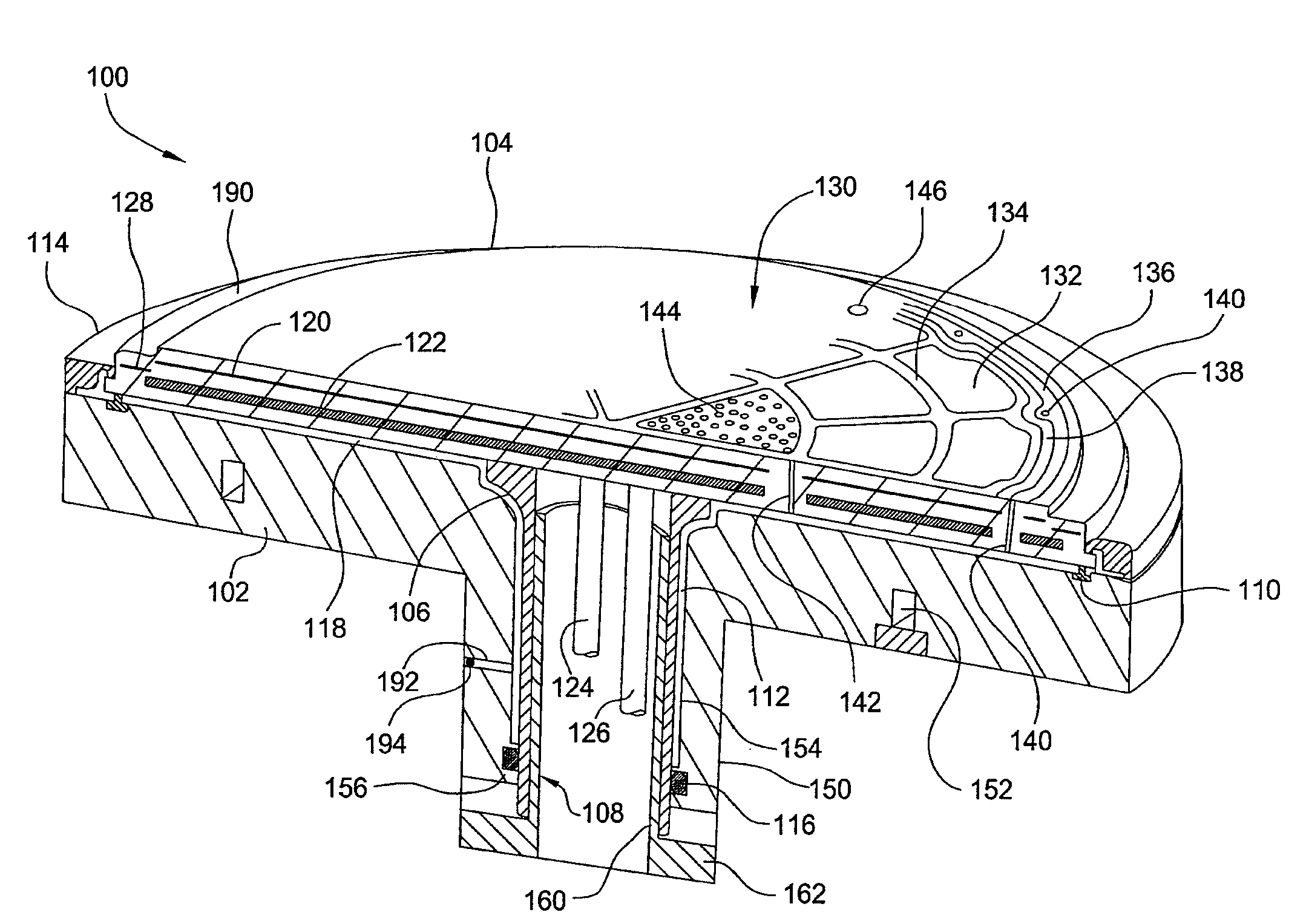
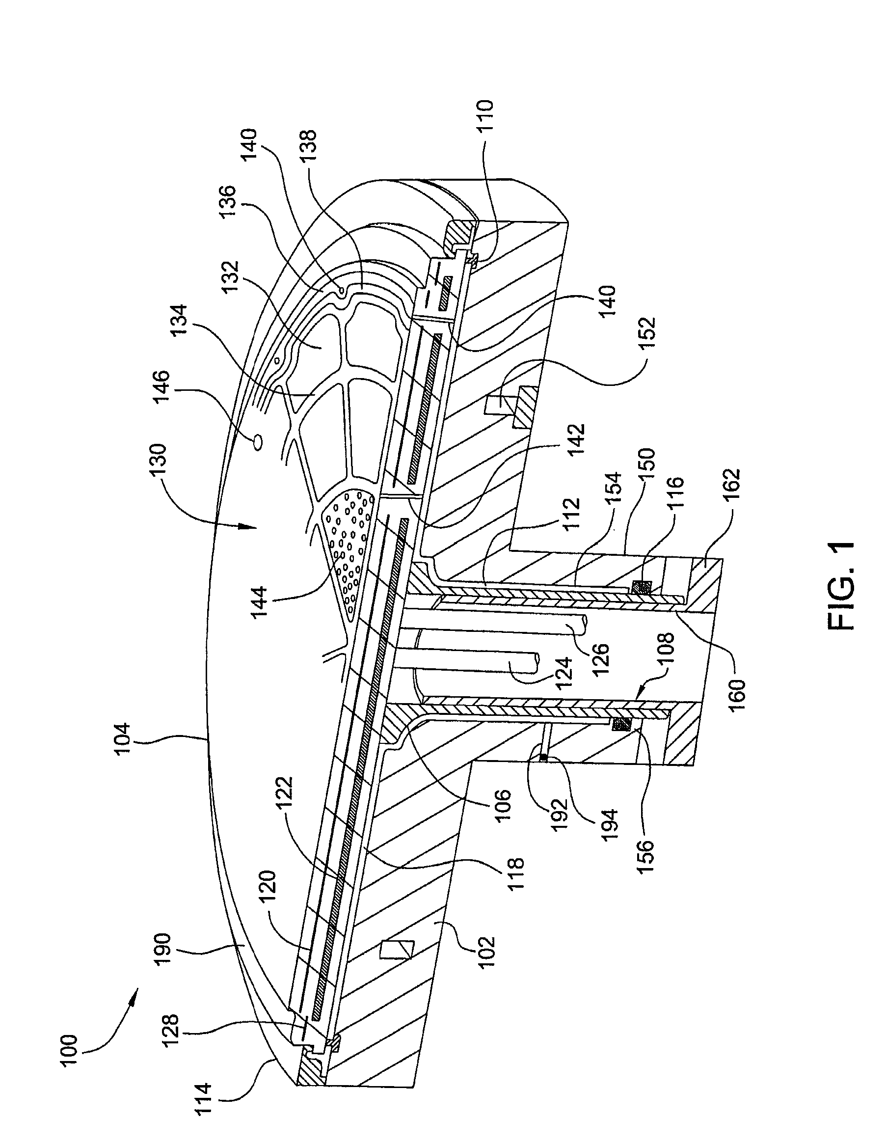
[0030]FIG. 1 is a sectional isometric view of one embodiment of a high temperature cathode 100 suitable for plasma etching. The cathode 100 may be advantageously utilized in plasma etch reactors, such as the AdvantEdge™ Etch reactor, available from Applied Materials, Inc., of Santa Clara, Calif., among other etch reactors, including suitable reactors available from other manufacturers.

[0031]FIG. 1 is one embodiment of a cathode 100. The cathode 100 generally includes an electrostatic chuck 104 secured to a cooling base 102. A stem 106 extends from a bottom of the electrostatic chuck 104. The stem 106 may be coupled to the electrostatic chuck 104 by braising or other suitable method. The stem 106 is generally fabricated from a conductive material such as stainless steel.

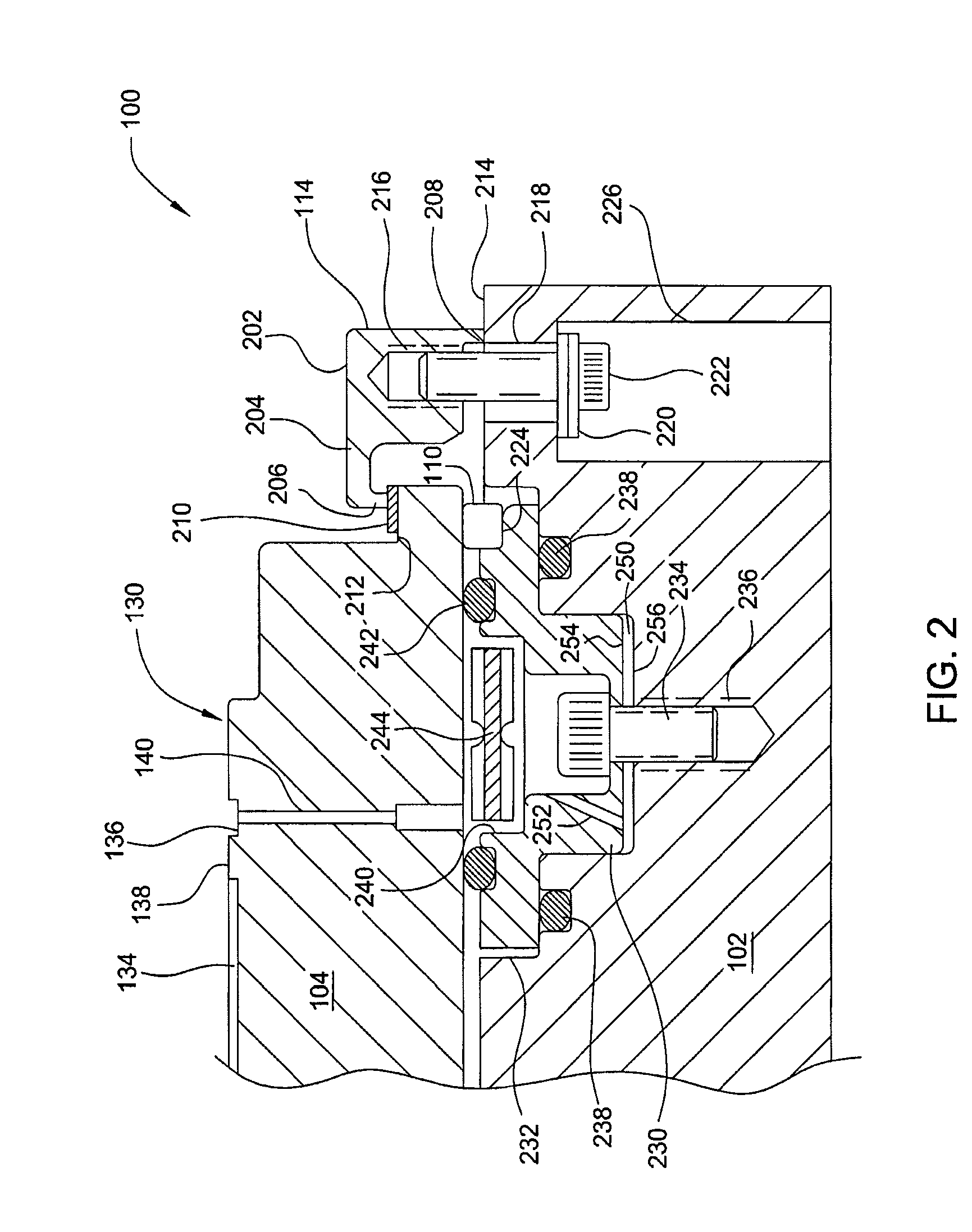
[0032]The electrostatic chuck 104 is supported above the cooling base 102 in a spaced-apart relation. In the embodiment depicted in FIG. 1, a support ring 110 is provided between the cooling base 102 and electrostatic...


PUM

PropertyMeasurementUnit
Diameteraaaaaaaaaa
Perimeteraaaaaaaaaa

Abstract

The present invention generally is a cathode suitable for use in high temperature plasma etch applications. In one embodiment, the cathode includes a ceramic electrostatic chuck secured to a base. The base has cooling conduits formed therein. A rigid support ring is disposed between the chuck and the base, thereby maintaining the chuck and the base in a spaced-apart relation.

Description

CROSS-REFERENCE TO RELATED APPLICATIONS[0001]This application claims benefit to U.S. Provisional Patent application Ser. No. 60 / 949,833, filed on Jul. 13, 2007.BACKGROUND[0002]1. Field of the Invention[0003]Embodiments of the present invention generally relate to semiconductor substrate processing systems. More specifically, the invention relates to a high temperature cathode suitable for plasma etching.[0004]2. Description of the Related Art[0005]In semiconductor wafer processing, the trend towards increasingly smaller feature size and linewidths have placed a premium on the ability to mask, etch, and deposit material on a semiconductor workpiece, or wafer, with greater precision. Plasma etching is of particular importance in obtaining critical dimensions less than 1.0 micron.[0006]Typically, plasma etching is accomplished by applying a RF power to a working gas supplied over a substrate held by a pedestal in a low pressure environment. The resulting electric field creates a reacti...

Claims


Application Information

Patent Timeline
IPC IPC(8): C25B11/02
CPCH01J37/20H01J37/32431H01L21/67069H01J2237/2001H01J2237/002H01L21/3065H01L21/205H01L21/02
Inventor YENDLER, BORISMATYUSHKIN, ALEXANDERKOOSAU, DENISEGAMI, GLEN
Owner APPLIED MATERIALS INC
Why Eureka
Try Eureka