Electronic component mounting system, electronic component placing apparatus, and electronic component mounting method

a technology for electronic components and mounting systems, applied in the direction of soldering apparatus, sustainable manufacturing/processing, final product manufacturing, etc., can solve the problems of poor conduction, easy occurrence of poor joints, so as to prevent poor joints

Active Publication Date: 2009-01-15
PANASONIC CORP
View PDF28 Cites 29 Cited by
  • Summary
  • Abstract
  • Description
  • Claims
  • Application Information

AI Technical Summary

Benefits of technology

[0021]According to the invention, whether the transfer of the solder paste to the solder bumps is necessary or not is judged on the basis of the measurement result of height of the solder paste, and in case that it is judged that the transfer is necessary, the tra

Problems solved by technology

Therefore, the solder bumps float due to the warp-deformation in the reflow time, and the solder bumps are not solder-joined normally

Method used


Image

  • Electronic component mounting system, electronic component placing apparatus, and electronic component mounting method
  • Electronic component mounting system, electronic component placing apparatus, and electronic component mounting method
  • Electronic component mounting system, electronic component placing apparatus, and electronic component mounting method

Examples


Embodiment Construction

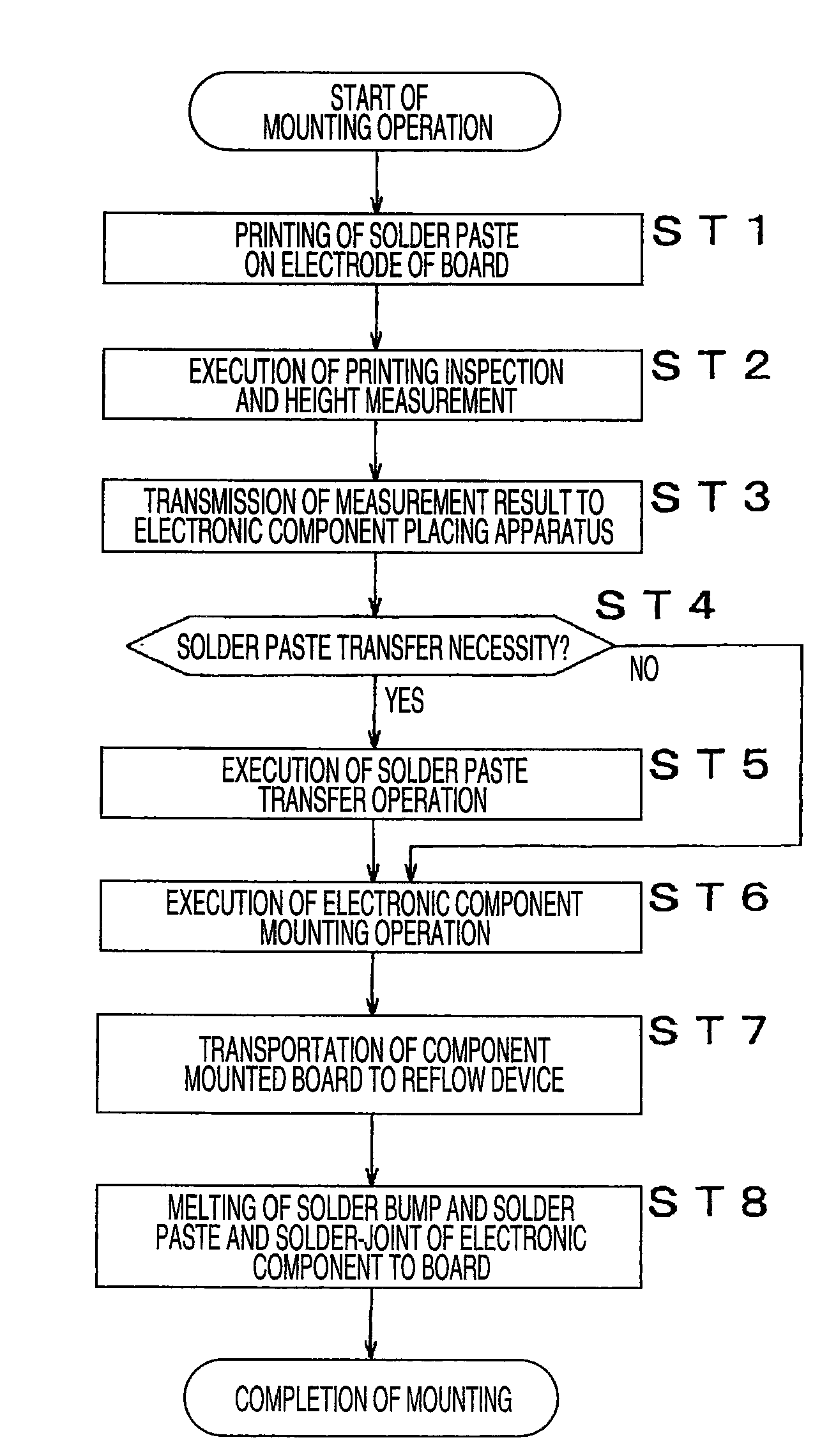
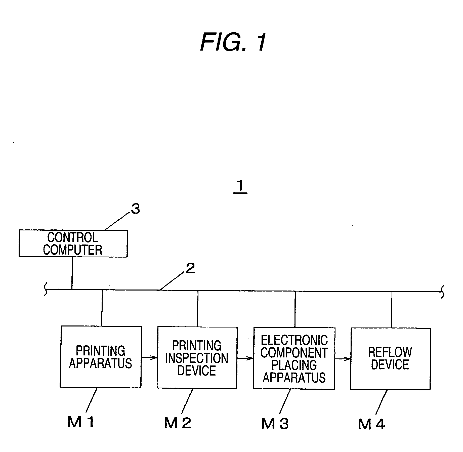
[0029]Next, an embodiment of the invention will be described with reference to drawings. Referring first to FIG. 1, the electronic component mounting system will be described. In the electronic component mounting system in FIG. 1, a printing apparatus M1, a printing inspection device M2, an electronic component placing apparatus M3, and a reflow device M4 all of which are electronic component mounting devices are coupled to constitute an electronic component mounting line 1, their devices are connected by a communication network 2, and the whole of the electronic component mounting system 1 is controlled by a control computer 3. In the embodiment, by these plural electronic component mounting devices, the electronic part having plural solder bumps for external connection on its surface is solder-joined to the board and mounted thereon, whereby a mounting board is manufactured.

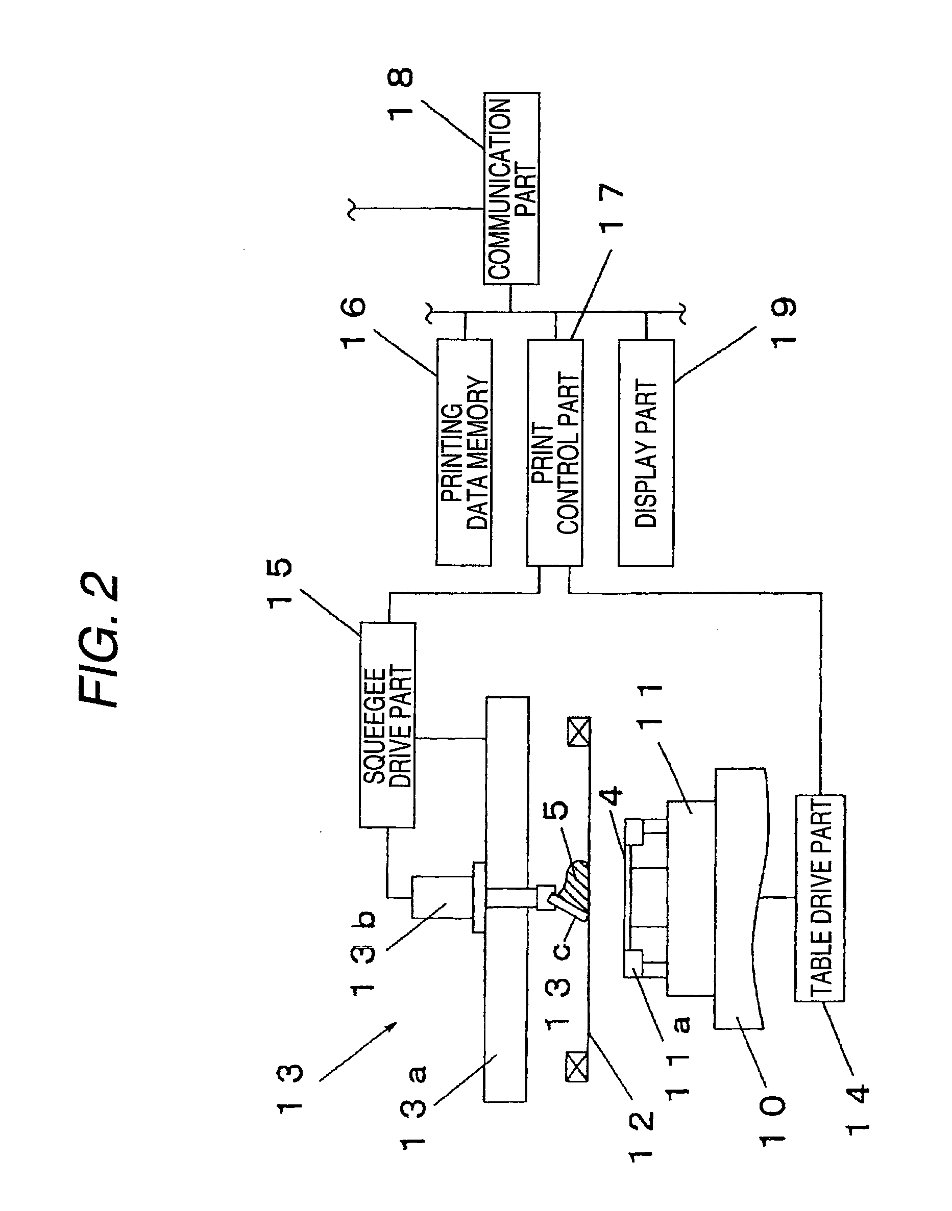
[0030]The printing apparatus M1 screen-prints, on electrodes formed on the board onto which the electronic c...


PUM

PropertyMeasurementUnit
Heightaaaaaaaaaa

Abstract

Regarding electronic component mounting in which an electronic component having plural solder bumps for external connection on its lower surface is mounted on a board, in an electronic component mounting operation of previously measuring the height position of solder paste on the board on which the solder paste has been printed, and mounting the electronic component on the board on which the solder paste has been printed by a loading head, whether the transfer of the solder paste to the solder bumps is necessary or not is judged on the basis of the measurement result of the height of the solder paste. In case that it is judged that the transfer is necessary, the transfer of the solder paste is executed, and thereafter the electronic component is mounted on the board. Hereby, it is possible to prevent the poor joint in case that a thin-sized semiconductor package which causes easily warp deformation is mounted on the board by solder-joint.

Description

TECHNICAL FIELD[0001]The present invention relates to an electronic component mounting system, an electronic component placing apparatus, and an electronic component mounting method, in which an electronic component on which solder bumps are formed is mounted on a board by solder-joint.BACKGROUND ART[0002]As a form of mounting an electronic component such as semiconductor element on a circuit board, a method of mounting a semiconductor package in which the semiconductor element is mounted on a resin board, on the circuit board through solder bumps by solder-joint has been used (refer to, for example, Patent Reference 1). In this referred example, an image of the lower surface of the package is picked up to recognize the solder bumps, whereby the bump arrangement and the positional shift of the bump are automatically detected, and data for judgment of the quality of the component and for positional correction are obtained.[0003][Patent Reference 1] JP-A-2000-315896DISCLOSURE OF THE I...

Claims


Application Information

Patent Timeline
IPC IPC(8): B23K31/12B23K1/20
CPCH05K1/0269H05K3/1216H05K3/3436H05K3/3484H05K13/0408H05K2203/163H05K13/08H05K2201/035H05K2201/10984H05K2203/0338H05K13/0465H01L2224/75H01L2224/81H01L2924/3511H05K13/0817H05K13/083H05K3/3485Y02P70/50B23K3/08H05K3/34H05K13/04B23K31/12
Inventor NISHI, SYOICHITSUKAMOTO, MITSUHAYAKIHARA, MASAHIROINOUE, MASAFUMI
Owner PANASONIC CORP
Why Eureka
Try Eureka