

Method of manufacturing bonded body for insulating circuit board, and bonded body for insulating circuit board
A manufacturing method and joint body technology, which can be used in the manufacture of printed circuits, the processing of insulating substrates/layers, and the manufacture of printed circuit precursors, etc., and can solve problems such as poor joints, inability to set guide posts, and imparting loads.
- Summary
- Abstract
- Description
- Claims
- Application Information
AI Technical Summary
Problems solved by technology
Method used
Image


Examples
Embodiment
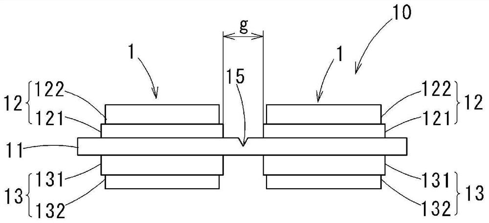
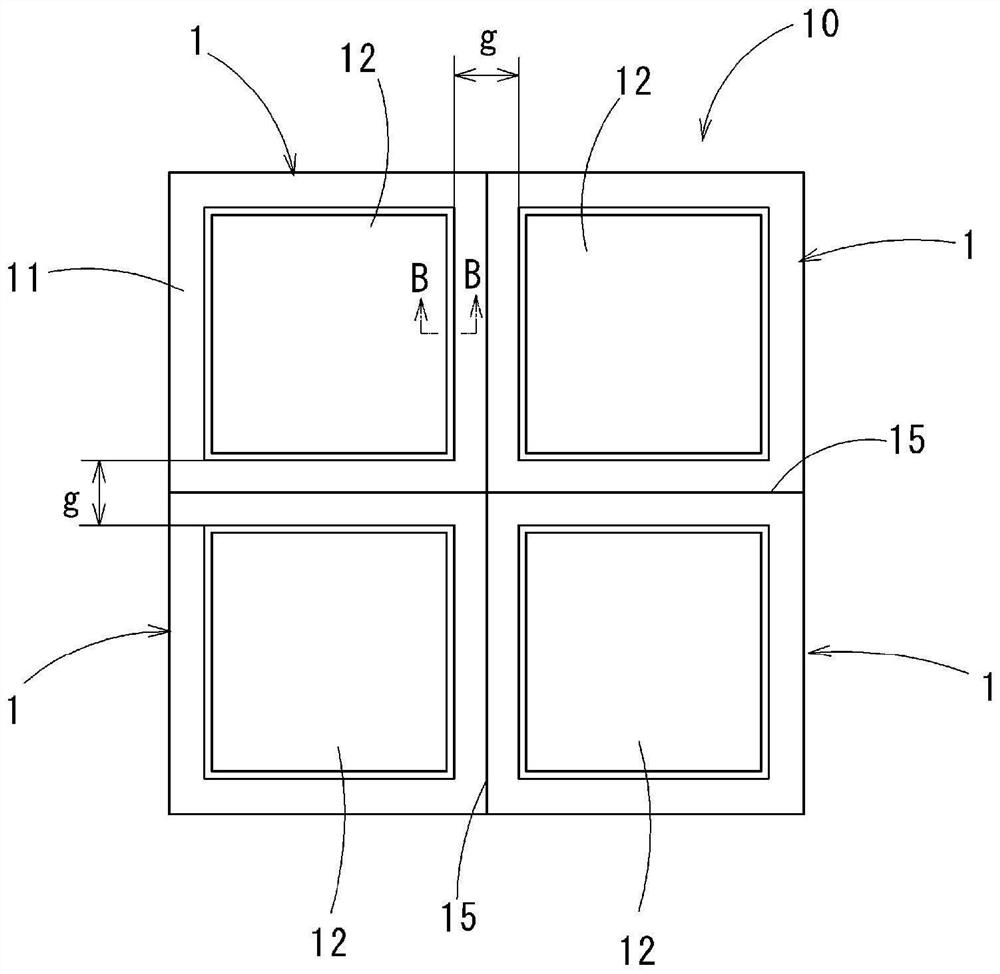
[0081] As an aluminum plate bonding process, two aluminum plates (38mm x 38mm, 4N-Al with a thickness of 0.25mm) are placed at a distance of 2mm on the surface of a ceramic substrate (40mm x 80mm, AlN with a thickness of 0.635mm) forming an insulating layer. For lamination, one aluminum plate (38 mm×78 mm, 4N-Al with a plate thickness of 0.25 mm) was laminated on the other surface of the ceramic substrate, and each was joined by brazing to form an aluminum layer. Al—Si brazing foil (thickness: 14 μm) was used as the brazing material, and a pressure of 0.3 MPa was applied in the lamination direction, and the temperature was heated at 640° C. for 40 minutes to join.
[0082] As the copper plate bonding process, a copper plate (37mm×37mm, thickness 0.3mm, oxygen-free copper) is positioned and stacked on the aluminum layer formed on the surface of the ceramic substrate, and on the aluminum layer formed on the back surface of the ceramic substrate , Laminate copper plates (37mm×77m...
PUM
| Property | Measurement | Unit |
|---|---|---|
| Radius of curvature | aaaaa | aaaaa |
Abstract
Description
Claims
Application Information