

Electronic component mounting method
A technology for electronic component installation and electronic components, which is applied in the direction of electrical components, electrical component assembly of printed circuits, electric solid devices, etc., can solve problems such as poor joints, poor electrical conductivity, and insufficient welding strength, and achieve the effect of preventing poor joints
- Summary
- Abstract
- Description
- Claims
- Application Information
AI Technical Summary
Problems solved by technology
Method used
Image

Examples
Embodiment Construction
[0015] Embodiments of the present invention are explained with reference to the drawings.
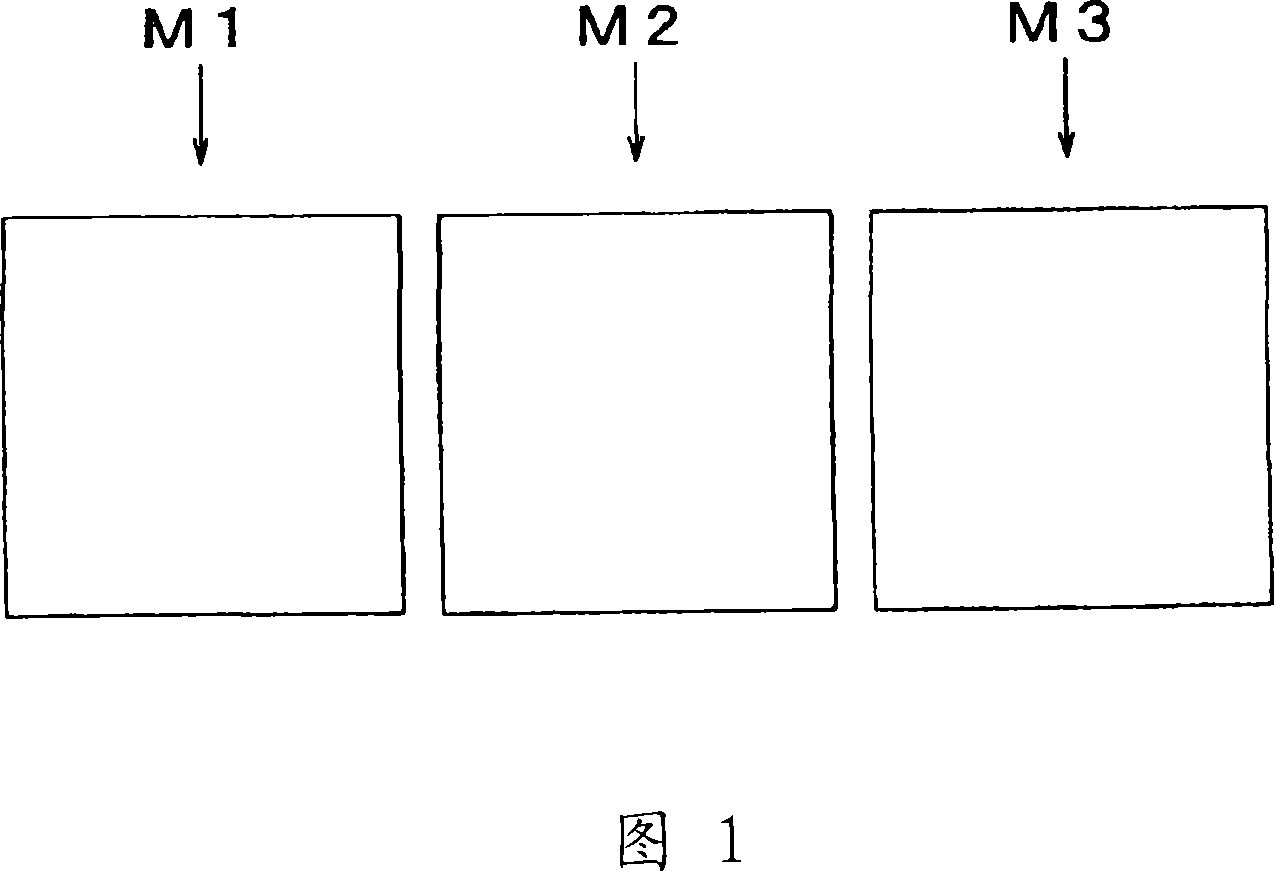
[0016] Referring first to Fig. 1, a component mounted board production line is explained. In FIG. 1, a component mounted board production line is configured to have a screen printer M1, an electronic component mounting device M2, and a reflow device M3 arranged in series. The screen printer M1 is used to print solder paste for attaching electronic components to the board. The electronic component placement device M2 is used for mounting electronic components on boards printed with solder paste. The reflow device M3 is used to heat the board on which the electronic components are mounted and fuse the solder component of the solder paste, thereby fixing the electronic components on the board.
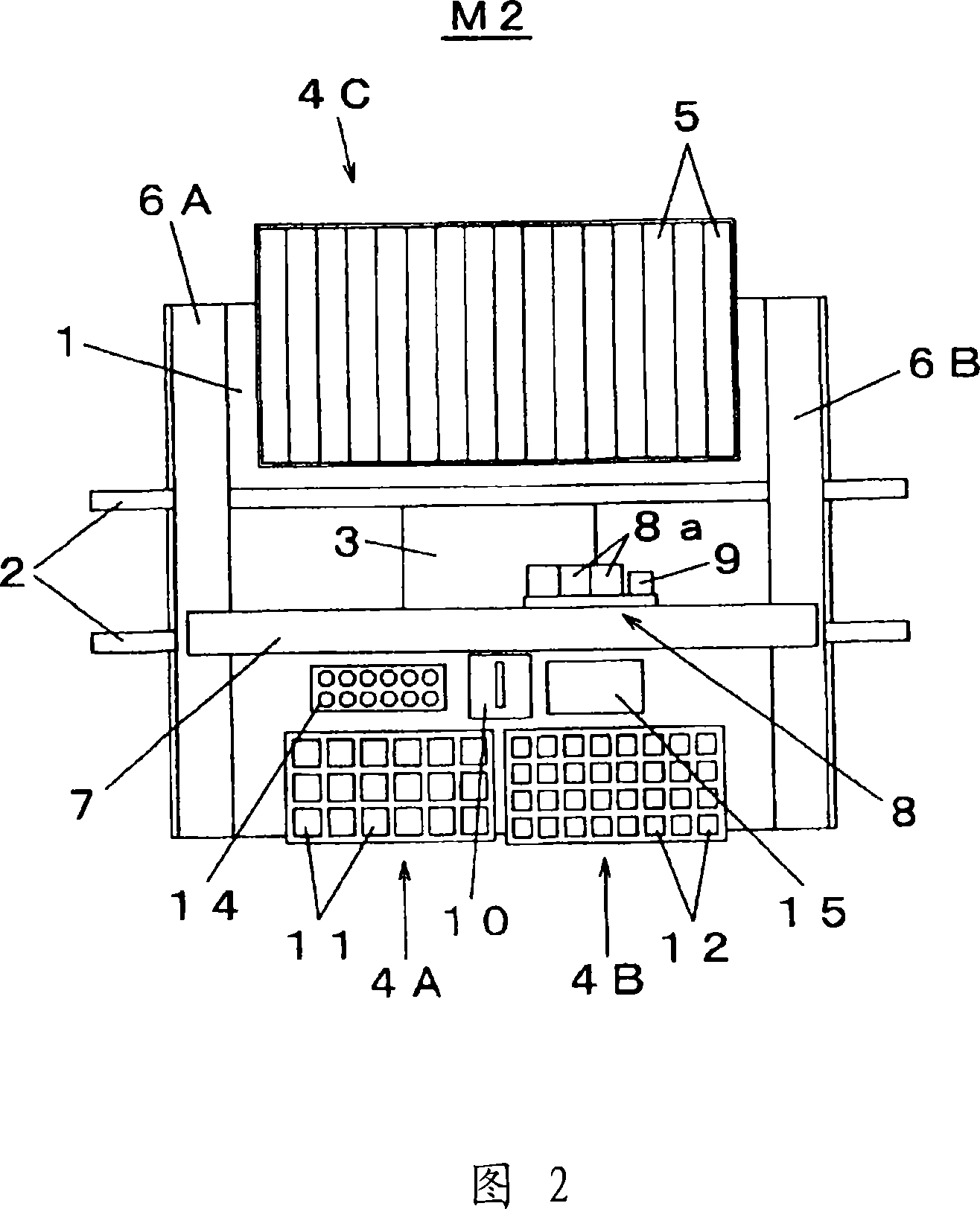
[0017] Referring now to FIG. 2, the construction of the electronic component mounting device M2 is explained. In FIG. 2 , the transport path 2 is arranged centrally in the base station 1 along t...
PUM
 Abstract
Description
Claims
Application Information