Chip package structure and manufacturing method thereof

A technology of chip packaging structure and manufacturing method, which is applied in semiconductor/solid-state device manufacturing, semiconductor/solid-state device parts, semiconductor devices, etc. Solve problems such as solid connection, to avoid cantilever deviation, avoid pin deformation, and avoid poor bonding of welding wires

Active Publication Date: 2013-01-23
CHIPMOS TECH INC
View PDF3 Cites 1 Cited by
  • Summary
  • Abstract
  • Description
  • Claims
  • Application Information

AI Technical Summary

Problems solved by technology

However, in the above-mentioned wire-bonding process, the cantilever part of the pin will shake or deform up and down due to the downward pressure, so that the soldering wire cannot be effectively fixed to the pin, so it is easy to fall off from the pin, resulting in poor electrical connection or failure
In addition, during the sealing process, the cantilever part of the pin is also easily shifted due to mold flow, resulting in pin bridge and electrical short circuit

Method used


Image

  • Chip package structure and manufacturing method thereof
  • Chip package structure and manufacturing method thereof
  • Chip package structure and manufacturing method thereof

Examples


Embodiment Construction

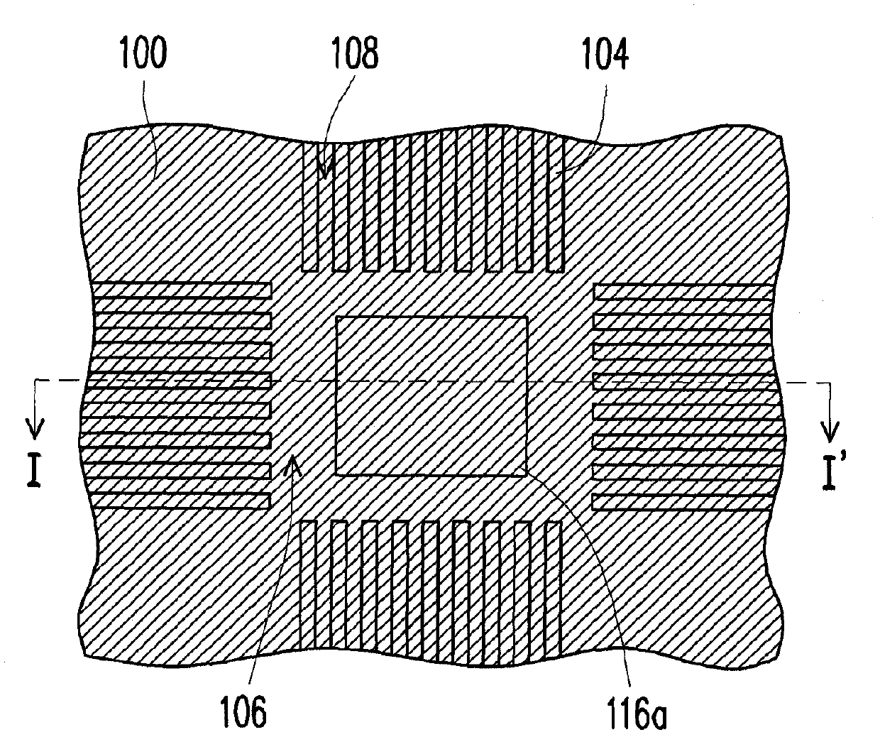
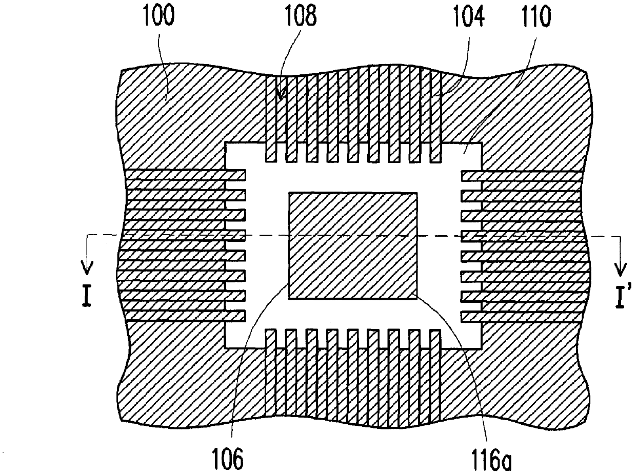
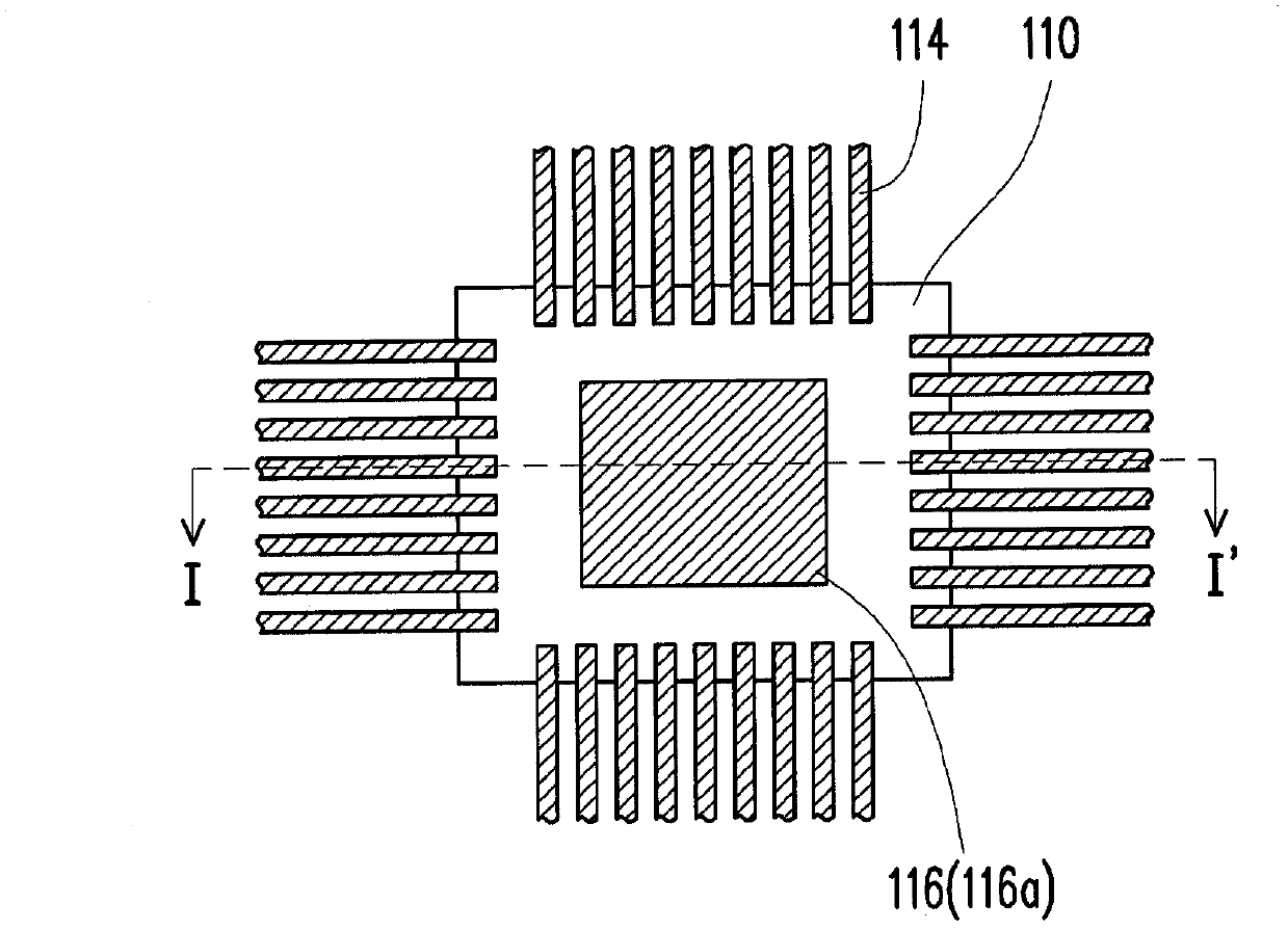
[0022] Figure 1A to Figure 1D It is a schematic top view of a method for manufacturing a chip package structure according to an embodiment of the present invention. Figure 2A to Figure 2D in accordance with Figure 1A to Figure 1D The cross-sectional schematic diagram shown by the section line I-I' in . First, please also refer to Figure 1A and Figure 2A , providing a metal layer 100 . The metal layer 100 has a first upper surface 100a and a first lower surface 100b opposite to the first upper surface 100a. The metal layer 100 is, for example, a copper foil substrate, which can be used to manufacture multiple lead frames. In this embodiment, only one lead frame is shown. Then, the first upper surface 100a of the metal layer 100 is patterned to define a chip bonding portion 116a and a plurality of lead portions 104, wherein there is a gap 106 between the lead portion 104 and the chip bonding portion 116a, and adjacent There are gaps 108 between the pin portions 104 . ...


PUM


Abstract

A chip package structure including a leadframe, a chip, bonding wires and an encapsulant is provided. The leadframe includes a die pad, leads and an insulating layer. The die pad includes a chip mounting portion and a periphery portion. At the periphery portion, the die pad has a second upper surface lying between a first upper surface and a lower surface of the die pad. Each lead includes a suspending portion and a terminal portion. The suspending portion connects to the terminal portion and extends from the terminal portion towards the die pad. The insulating layer is disposed on the second upper surface of the periphery portion and connects the suspending portions to the die pad. The chip is disposed on the chip mounting portion. The bonding wires electrically connect the chip to the suspending portions. The encapsulant covers the chip, the bonding wires, the insulating layer, and the leadframe.

Description

technical field [0001] The present invention relates to a semiconductor packaging technology, and in particular to a chip packaging structure and a manufacturing method thereof. Background technique [0002] Semiconductor packaging technology includes many packaging forms. With the trend of miniaturization and thinning of the chip package structure, a quad flat no-lead (QFN) package belonging to the flat package series has been developed. In the quad flat no-lead package process, the chip is usually placed on the chip pad in the lead frame first. Then, a wire bonding process is performed, so that the chip is electrically connected to pins in the lead frame through a plurality of bonding wires. Afterwards, the chip, bonding wires, and lead frame are covered by encapsulant. [0003] Generally, the above-mentioned leads include a cantilever portion, so that the encapsulant can be filled under the cantilever portion, which helps the mold lock of the encapsulant and the lead t...

Claims


Application Information

Patent Timeline
Patent Type & Authority Applications(China)
IPC IPC(8): H01L23/495H01L21/31H01L21/60H01L21/56
CPCH01L2224/32245H01L21/565H01L23/49548H01L2224/73265H01L2224/48247H01L21/4828H01L23/49558H01L23/3107H01L21/4825H01L23/49503H01L24/73H01L2924/00012
Inventor 潘玉堂周世文
Owner CHIPMOS TECH INC
Why Eureka
Try Eureka