Three-dimensional die-stacking package structure and method for manufacturing the same

Active Publication Date: 2009-01-15
IND TECH RES INST
View PDF9 Cites 66 Cited by
  • Summary
  • Abstract
  • Description
  • Claims
  • Application Information

AI Technical Summary

Benefits of technology

[0010]According to the present invention, the bottom electrode of the top substrate is intended for the electroplating of the bottom opening of the three-dimensional die-stacking package st

Problems solved by technology

To make it, one of the challenging tasks facing the industry is to perform high aspect ratio drilling as well as high aspect ratio blind via plating.
However, expensive equipments are always required to form the bottom metal electrode or the silicon dioxide insulating layer under the chemi

Method used


Image

  • Three-dimensional die-stacking package structure and method for manufacturing the same
  • Three-dimensional die-stacking package structure and method for manufacturing the same
  • Three-dimensional die-stacking package structure and method for manufacturing the same

Examples


first embodiment

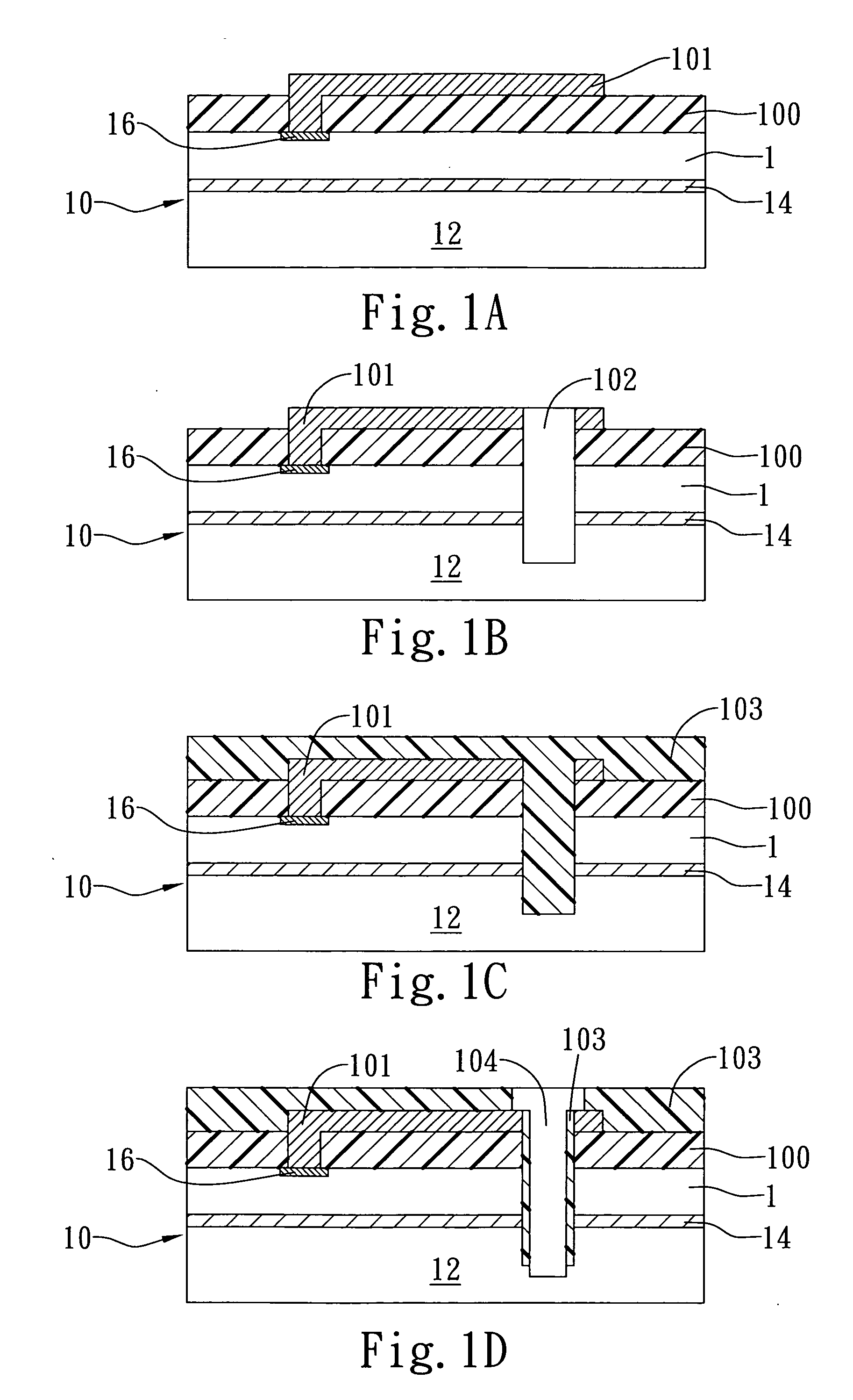
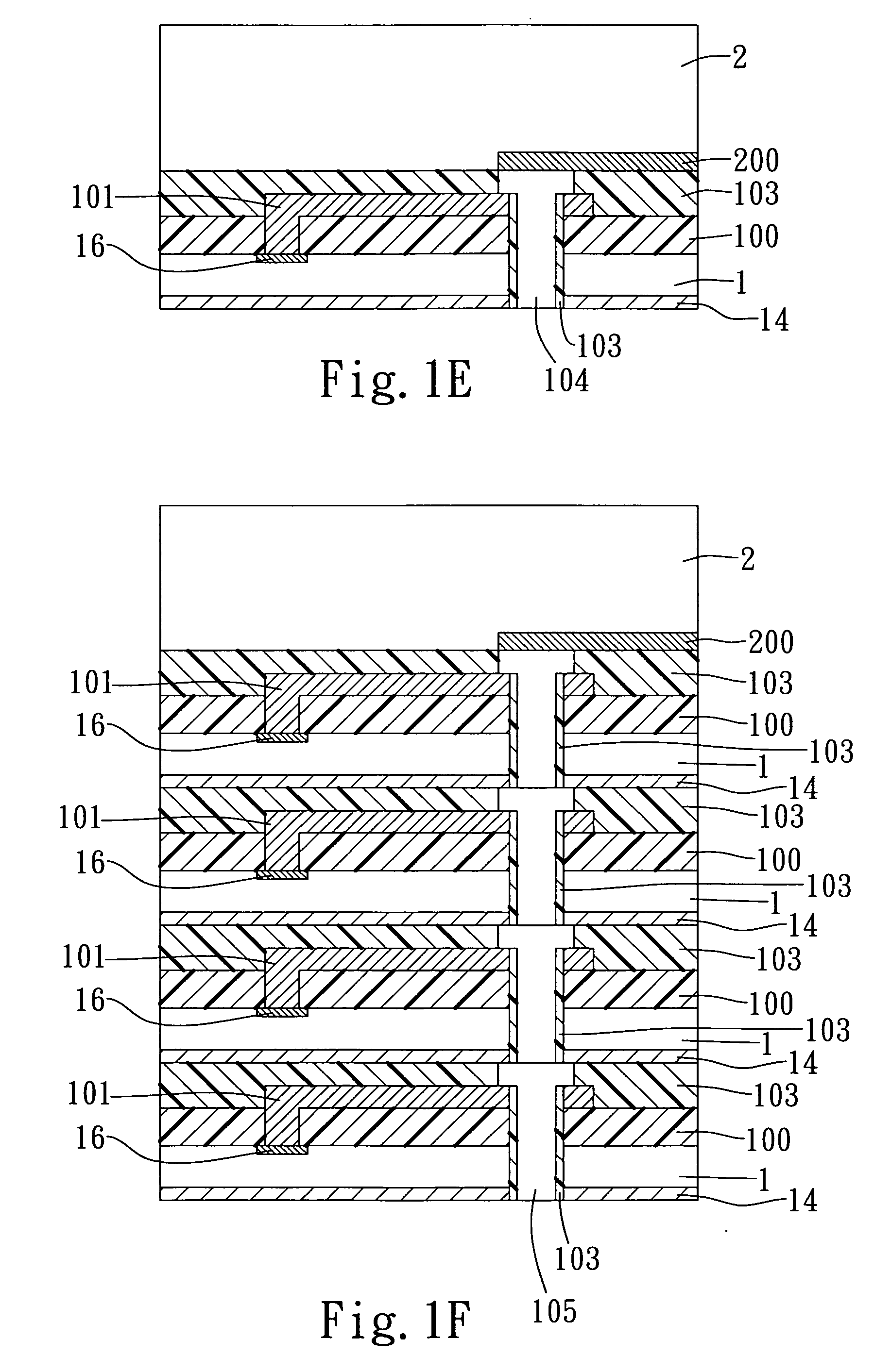
[0018]A variance of the method for manufacturing a three-dimensional die-stacking package structure according to the present invention begins with the completion of the manufacture of the multiple respective SOI wafers 10 each of which containing a plurality of IC dice 1 on the insulating layer 14 and the polymer insulating layer 100 on the surface of the SOI wafer 10 opposite to the insulating layer 14, followed by taking the polymer insulating layer 103 on the polymer insulating layer 100 of each SOI wafer 10 as an adhering layer in between to stack such SOI wafers 10 together in a back-to-face manner and in a way that every single SOI wafer 10 sits in the prescribed direction on the upper side of the following one, wherein the insulating layer 14 of each SOI wafer 10 is jointed to the polymer insulating layer 103 of the following one. Then, the top substrate 2 is stacked atop the polymer insulating layer 103 of the topmost SOI wafer, so as to produce a wafer level three-dimension...

second embodiment

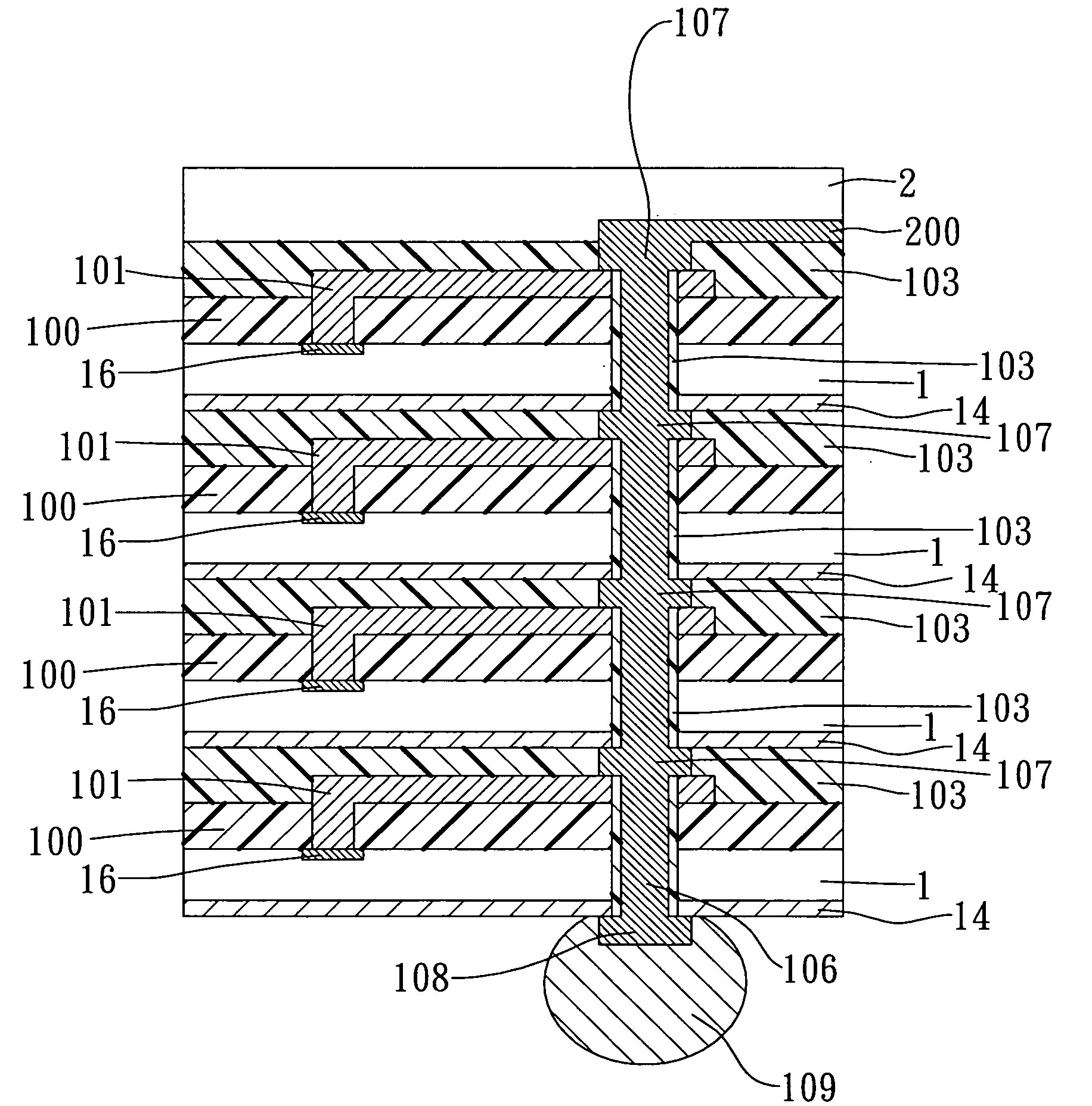
[0019]FIG. 2 shows a cross-sectional view of the three-dimensional die-stacking package structure of the present invention. It should be noted that layers in FIG. 2 correspond to those with the same reference numbers in FIG. 1G. In this embodiment, the top substrate 2 is stacked on a backside of the aforementioned SOI wafer 10 that contains a plurality of IC dice 1 on the insulating layer 14 thereof. The three-dimensional die-stacking package structure comprises, but not limited to, four die units stacked together in a face-to-back manner with a top substrate 2 stacked on the backside of the topmost die unit. More specifically, every die unit uses the polymer insulating layer 103 on its upper side to join the insulating layer 14 on the backside of its following die unit, with its first metal contact pad 107 electrically connected to the bottom of the metal contact 106 of its following die unit. Moreover, the bottom electrode 200 of the top substrate 2 is electrically connected to th...


PUM


Abstract

This invention provides a substrate having at least one bottom electrode formed therein. A plurality of dice each having at least one opening formed therein are vertically stacked together one by one by a polymer insulating layer acting as an adhering layer between them, along with the openings thereof aligned to each other to form a through hole passing through said dice. The stacked dice are joined to a bottom of the substrate with the polymer insulating layer acting as an adhering layer, making the bottom electrode of the substrate contact the through hole. An electroplating process is performed with the bottom electrode serving as an electroplating electrode to form a conductive contact passing through the dice.

Description

BACKGROUND OF THE INVENTION[0001]1. Field of the Invention[0002]The present invention relates to a three-dimensional die-stacking package structure and a method for manufacturing the same; and more particularly to a wafer level three-dimensional die-stacking package structure and a method for manufacturing the same.[0003]2. Description of the Related Art[0004]Because the three-dimensional die-stacking package structure has short signal transmission distance, the three-dimensional die-stacking package structure has always had high performance in telecommunications and been applicable to quality package structures of high-speed devices. By being vertically stacked, the three-dimensional die-stacking package structure is also able to significantly reduce its size to meet the slim and compact trend in the industry and to multiply its memory capacity under given package size in terms of memory packaging. One of the major technique features involved in the process of the three-dimensional...

Claims


Application Information

Patent Timeline
IPC IPC(8): H01L23/498H01L21/60
CPCH01L21/6835H01L24/27H01L24/24H01L24/29H01L24/94H01L25/0657H01L25/50H01L2221/68359H01L2221/68377H01L2224/16H01L2224/24145H01L2224/274H01L2224/32188H01L2224/9202H01L2225/06513H01L2225/06527H01L2225/06541H01L2924/01078H01L2924/14H01L2924/15311H01L2224/2919H01L2924/01033H01L2924/014H01L2924/0665H01L2224/29101H01L21/76898H01L2924/00H01L2224/05024H01L2224/02372H01L2224/05008H01L2224/05026H01L2224/13025H01L2224/05001H01L2224/056H01L2924/00014H01L2224/32145H01L24/03H01L24/06H01L24/05H01L2224/92144H01L24/02H01L2224/05099
Inventor CHANG, HSIANG-HUNGCHANG, SHU-MING
Owner IND TECH RES INST
Why Eureka
Try Eureka