Forming submicron integrated-circuit wiring from gold, silver, copper, and other metals

a technology of integrated circuit wiring and metals, applied in the direction of electrical equipment, semiconductor devices, semiconductor/solid-state device details, etc., can solve the problems of inability to planarize, inability to meet the requirements of micron and submicron metallization, so as to preserve the insulative and capacitance-reducing properties of polymeric insulators, reduce the reaction with metals, and increase the conductivity of poly

Inactive Publication Date: 2005-02-01
ROUND ROCK RES LLC
View PDF78 Cites 23 Cited by
  • Summary
  • Abstract
  • Description
  • Claims
  • Application Information

AI Technical Summary

Benefits of technology

Moreover, in another embodiment, the invention applies this liftoff technique to form silver, gold, and copper conductors in a polymeric insulator formed and cured using a unique procedure that reduces reactions with metals, particularly copper. The new procedure preserves the insulative and capacitance-reducing properties of the polymeric insulator. In contrast, conventional polymer processing techniques promote the formation of conductive oxides which increase the conductivity of the polymer and thus undermines its insulative and capacitance-reducing properties. Thus, the present invention facilitates the fabrication of integrated circuits with superior speed, efficiency, and reliability.

Problems solved by technology

Without this distinct break, lifting the mask pulls and breaks or otherwise damages the microscopic metal structures—the wires—deposited on the insulative layer.
Ensuring this distinct break, which conventionally requires building a thick mask having openings with steep, high sidewalls, is thought impractical for micron and submicron metallization because of difficulties in forming thick masks with steep-walled micron and submicron openings.
These difficulties stemmed principally from inadequate planarization techniques, photolithographic limitations, and etching-control problems.

Method used


Image

  • Forming submicron integrated-circuit wiring from gold, silver, copper, and other metals
  • Forming submicron integrated-circuit wiring from gold, silver, copper, and other metals
  • Forming submicron integrated-circuit wiring from gold, silver, copper, and other metals

Examples


Embodiment Construction

The following detailed description, which references and incorporates FIGS. 1-10, describes and illustrates one or more specific embodiments of the invention. These embodiments, offered not to limit but only to exemplify and teach the invention, are shown and described in sufficient detail to enable those skilled in the art to practice the invention. Thus, where appropriate to avoid obscuring the invention, the description may omit certain information known to those of skill in the art.

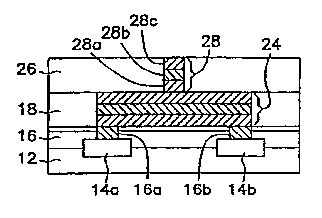
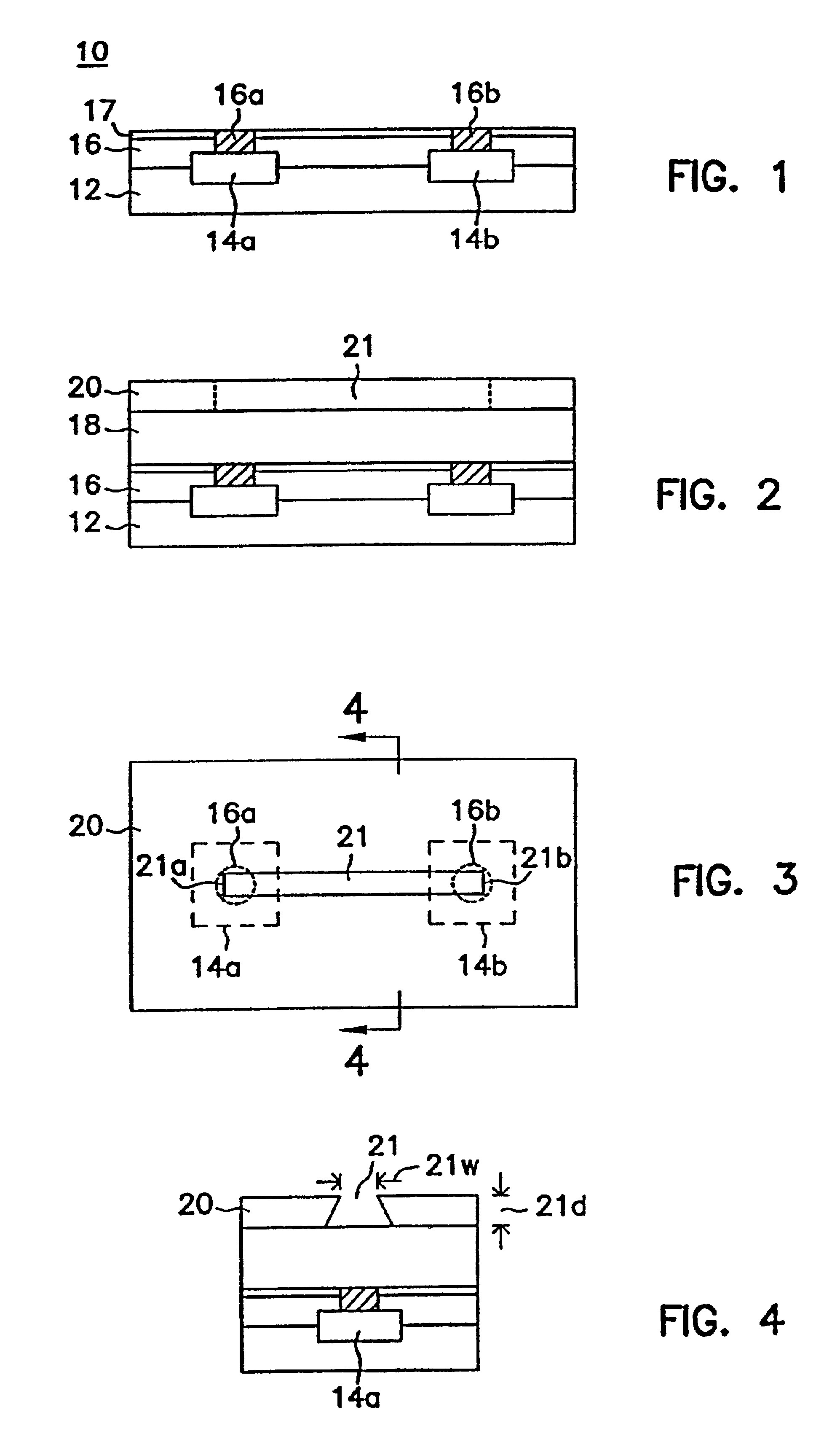
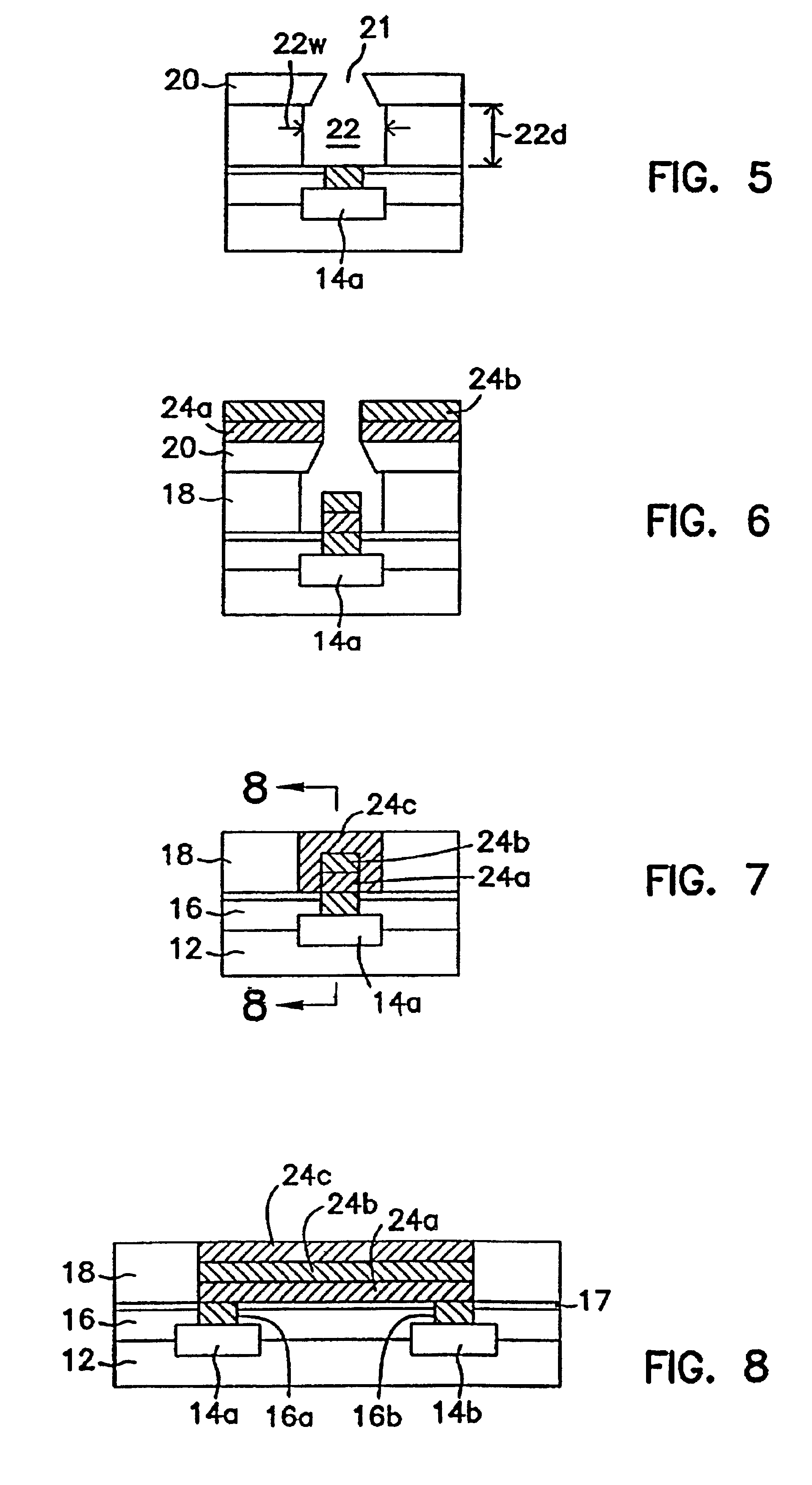
FIGS. 1-9 show a number of exemplary integrated-circuit assemblies, which taken collectively and sequentially, illustrate an exemplary method of the present invention. The method, as shown in FIG. 1, a cross-sectional view, begins with a known integrated-circuit assembly or structure 10, which can be within any integrated circuit, an integrated memory circuit, for example. Assembly 10 includes a substrate 12. The term “substrate,” as used herein, encompasses a semiconductor wafer as well as structures...


PUM

PropertyMeasurementUnit
widthaaaaaaaaaa
thickaaaaaaaaaa
widthaaaaaaaaaa

Abstract

A typical integrated circuit interconnects millions of microscopic transistors and resistors with aluminum wires buried in silicon-dioxide insulation. Yet, aluminum wires and silicon-dioxide insulation are a less attractive combination than gold, silver, or copper wires combined with polymer-based insulation, which promise both lower electrical resistance and capacitance and thus faster, more efficient circuits. Unfortunately, conventional etch-based techniques are ineffective with gold, silver, or copper, and conventional polymer formation promote reactions with metals that undermine the insulative properties of polymer-based insulations. Accordingly, the inventor devised methods which use a liftoff procedure to avoid etching problems and a non-acid-polymeric precursor and non-oxidizing cure procedure to preserve the insulative properties of the polymeric insulator. The resulting interconnective structures facilitate integrated circuits with better speed and efficiency.

Description

FIELD OF INVENTIONThe present invention concerns methods of fabricating integrated circuits, particularly methods of forming integrated-circuit wiring, or interconnects, from metals, such as gold, silver, and copper.BACKGROUND OF THE INVENTIONIntegrated circuits, the key components in thousands of electronic and computer products, are interconnected networks of electrical components fabricated on a common foundation, or substrate. Fabricators typically use various techniques, such as layering, doping, masking, and etching, to build thousands and even millions of microscopic resistors, transistors, and other electrical components on a silicon substrate, known as a wafer. The components are then wired, or interconnected, together to define a specific electric circuit, such as a computer memory.Interconnecting millions of microscopic components typically follows one of two different methods, both of which initially entail covering the components with an insulative layer. In the first m...

Claims


Application Information

Patent Timeline
Patent Type & Authority Patents(United States)
IPC IPC(8): H01L23/532H01L21/70H01L23/52H01L21/768
CPCH01L21/76802H01L21/76843H01L21/76874H01L21/76879H01L23/53228H01L23/53238H01L23/53242H01L23/53252H01L23/5329H01L2924/0002H01L2924/00
Inventor FARRAR, PAUL A.
Owner ROUND ROCK RES LLC
Why Eureka
Try Eureka