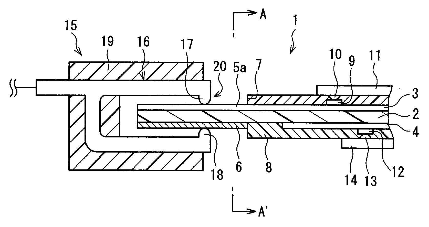
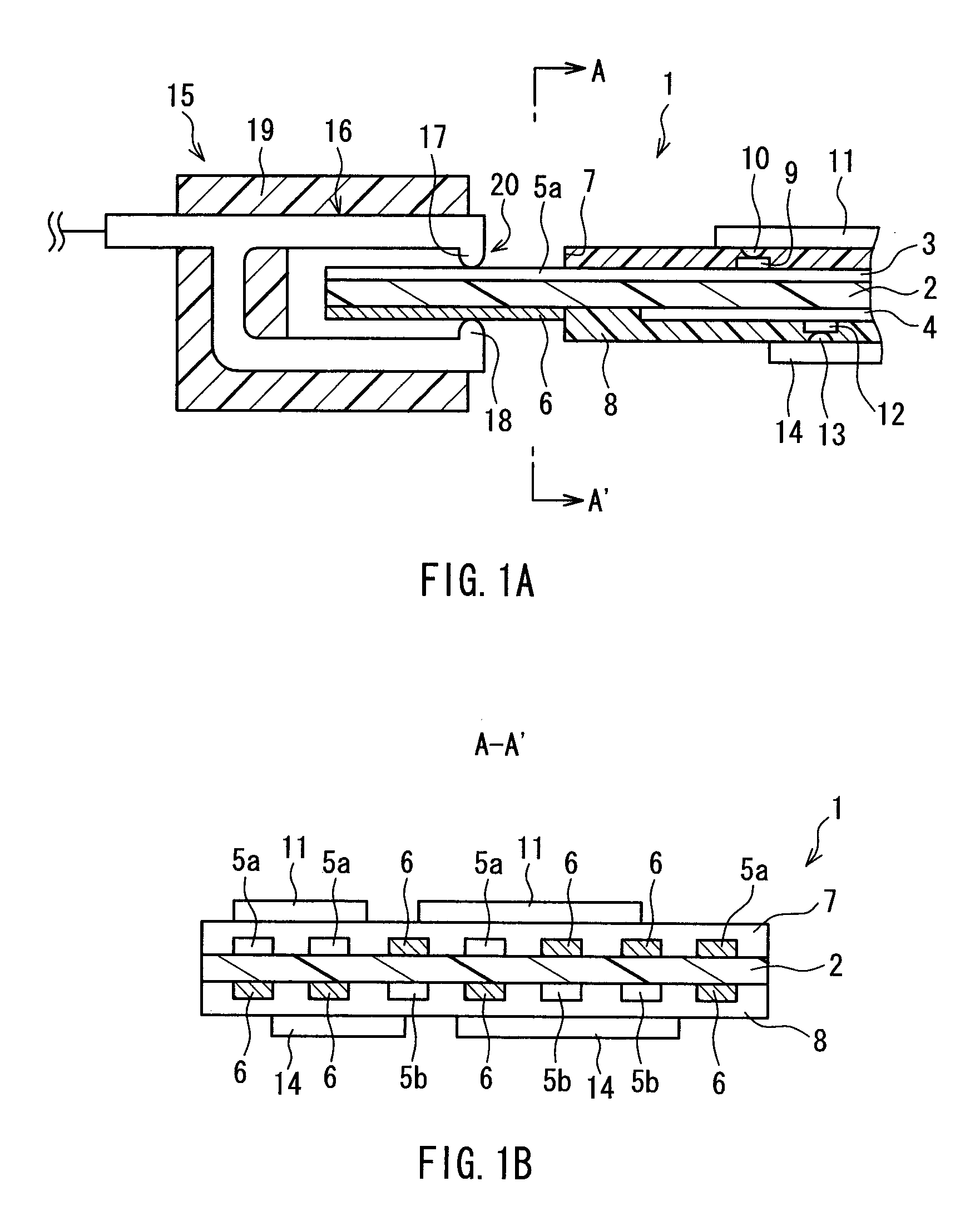
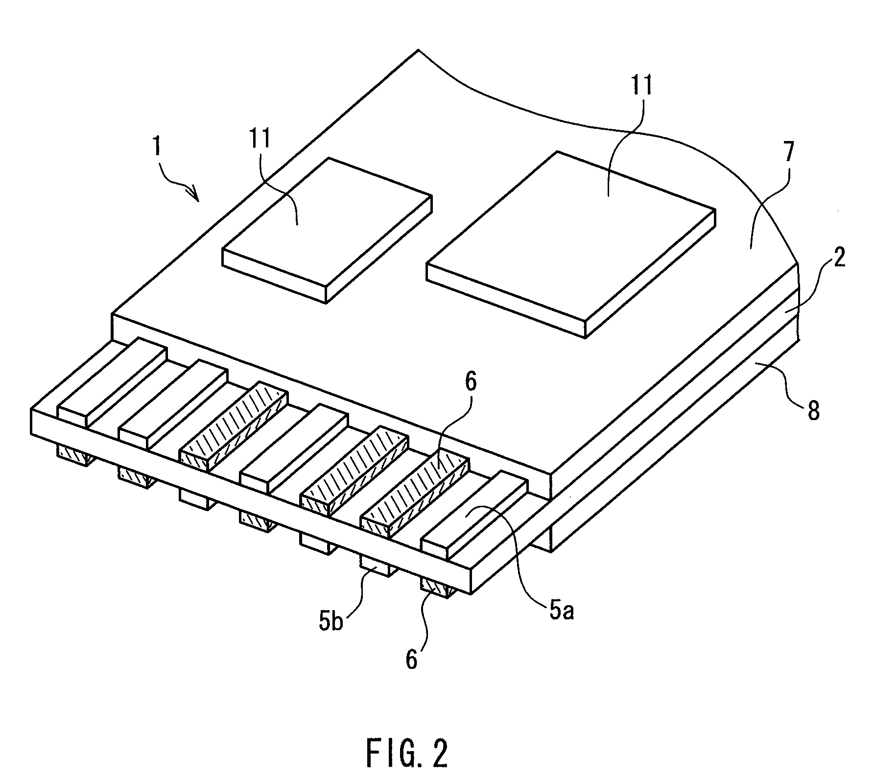
[0033]A circuit board according to a preferred embodiment of the present invention is connected to a connector that includes a connection port for receiving an object to be connected and a plurality of contact portions located at upper and lower positions of the connection port. Any of the contact portions at one of the upper and lower positions and any of the contact portions at the other position face each other in a vertical direction, and each contact portion is connected electrically to the opposite contact portion. The circuit board includes a base substrate, a first wiring layer formed on one principal surface of the base substrate, and a second wiring layer formed on the other principal surface of the base substrate. First terminals connected to the first wiring layer are provided on the one principal surface, and second terminals connected to the second wiring layer are provided on the other principal surface. The first terminals and the second terminals come into contact with any of the contact portions and are arranged so as not to overlap each other in the vertical direction.
[0034]A connection structure according to a preferred embodiment of the present invention includes a connector and a circuit board. The connector and the circuit board are connected to form the connection structure. The connector includes a connection port for receiving the circuit board and a plurality of contact portions located at upper and lower positions of the connection port. Any of the contact portions at one of the upper and lower positions and any of the contact portions at the other position face each other in a vertical direction, and each contact portion is connected electrically to the opposite contact portion. The circuit board includes a base substrate, a first wiring layer formed on one principal surface of the base substrate, and a second wiring layer formed on the other principal surface of the base substrate. First terminals connected to the first wiring layer are provided on the one principal surface, and second terminals connected to the second wiring layer are provided on the other principal surface. The first terminals and the second terminals come into contact with any of the contact portions and are arranged so as not to overlap each other in the vertical direction.
[0035]In the circuit board and the connection structure according to a preferred embodiment of the present invention, it is preferable that dummy terminals that are insulated electrically from the first wiring layer and the second wiring layer are provided on both principal surfaces of the base substrate, and the dummy terminals are located in a region that is on the opposite side of the base substrate to a region where the first terminals or the second terminals are provided. With this configuration, the thicknesses of portions of the circuit board that come into contact with the connector can be uniform, and the connection between the circuit board and the connector can be stabilized.
[0036]The circuit board and the connection structure according to various preferred embodiments of the present invention are useful when the base substrate has flexibility, and the circuit board is a flexible printed circuit board. In the circuit board and the connection structure according to various preferred embodiments of the present invention, electronic components may be mounted on the one principal surface so as to be connected electrically to the first wiring layer, and different electronic components from those electronic components may be mounted on the other principal surface so as to be connected electrically to the second wiring layer.
[0037]According to another preferred embodiment, an apparatus of the present invention includes the connection structure of the present preferred embodiment of the present invention.
[0038]Hereinafter, a circuit board, a connection structure, and an apparatus according to a preferred embodiment of the present invention will be described with reference to FIGS. 1A to 4.
[0039]First, the circuit board and the connection structure of this embodiment will be described by referring to FIGS. 1A to 3. FIGS. 1A and 1B are cross-sectional views showing the circuit board and the connection structure of this preferred embodiment. FIG. 1A is a cross-sectional view of the connection structure. FIG. 1B is a cross-sectional view of the circuit board taken along the line A-A′ in FIG. 1A. FIG. 2 is a perspective view showing the appearance of the circuit board in FIG. 1. FIG. 3 is a perspective view showing the appearance of a connector that constitutes the connection structure in FIG. 1. In FIGS. 1A and 1B, the cross section of a conductive member (except for a dummy terminal 6) is not hatched, and electronic components are shown only in outline.
[0040]As shown in FIG. 1A, the connection structure includes a circuit board 1 and a connector 15 and is formed by connecting the circuit board 1 to the connector 15. In this case, the connector 15 is a dual contact connector, which is similar to the connector 40 in FIG. 5 as described in Background Art.
[0041]As shown in FIGS. 1A and 3, the connector 15 includes a connection port 20 into which the circuit board 1 (i.e., an object to be connected) is inserted, a plurality of contact portions 17 located at the upper position of the connection port 20, and a plurality of contact portions 18 located at the lower position of the connection port 20. The contact portions 17 face any of the contact portions 18 in the vertical direction and are connected electrically to the opposite contact portions 18.
[0042]In the context of the present invention, the vertical direction indicates a direction that is the same as the thickness direction of the circuit board 1 when it is inserted into the connection port 20 of the connector 15. The upper position of the connection port 20 indicates the side facing the upper surface of the circuit board 1 when it is inserted into the connection port 20. The lower position of the connection port 20 indicates the side facing the lower surface of the circuit board 1 when it is inserted into the connection port 20.
[0043]In this preferred embodiment, the connector 15 includes a plurality of terminal members 16 made of a conductive material and a housing 19 made of a resin material. Each of the terminal members 16 preferably has a substantially U-shaped portion, and one end of the substantially U-shaped portion is the contact portion 17 and the other end of the substantially U-shaped portion is the contact portion 18.
[0044]As shown in FIG. 3, the terminal members 16 are arranged by the housing 19 along the direction that is substantially perpendicular to the insertion direction of the circuit board 1 so that the contact portions 17 are located opposite the respective contact portions 18 in the vertical direction. Therefore, the contact portions 17, 18 facing each other in the vertical direction are connected electrically. Moreover, the contact portions 17, 18 are aligned respectively in a line along the direction that is substantially perpendicular to the insertion direction of the circuit board 1.
[0045]As shown in FIGS. 1B and 2, the circuit board 1 includes a base substrate 2, a first wiring layer 3 formed on one principal surface of the base substrate 2, and a second wiring layer 4 formed on the other principal surface of the base substrate 2.
[0046]In this preferred embodiment, the first wiring layer 3 and the second wiring layer 4 have signal conductors, respectively. The first wiring layer 3 and the second wiring layer 4 are not a shielding layer. The circuit board 1 is a FPC board, and the base substrate 2 is made of a resin film with flexibility such as a polyester film, polyamide film, or polyimide film. Reference numeral 7, 8 denote a protective film made of a resin material. In preferred embodiments of the present invention, the circuit board may be a rigid board.
[0047]As shown in FIGS. 1B and 2, a plurality of first terminals 5a in the form of stripes are provided on the principal surface on which the first wiring layer 3 is formed. Also, a plurality of second terminals 5b in the form of stripes are provided on the principal surface on which the second wiring layer 4 is formed. Moreover, the first terminals 5a and the second terminals 5b are arranged so as to come into contact with any of the contact portions 17, 18 of the connector 15.
[0048]In this preferred embodiment, the protective film 7 is formed not to cover a portion of the first wiring layer 3, and the portion that is not covered with the protective film 7 corresponds to the first terminal 5a. Similarly, the protective film 8 is formed not to cover a portion of the second wiring layer 4, and the portion that is not covered with the protective film 8 corresponds to the second terminal 5b.
[0049]The first terminals 5a and the second terminals 5b are arranged so as to come into contact with any of the contact portions 17, 18 of the connector 15. Moreover, as shown in FIGS. 1B and 2, the first terminals 5a and the second terminals 5b do not overlap in the vertical direction. In this preferred embodiment, a plurality of dummy terminals 6 are provided in a region that is on the opposite side of the base substrate 2 to a region where the first terminals 5a or the second terminals 5b are arranged. The dummy terminals 6 are arranged so as to overlap the first terminals 5a or the second terminals 5b in the vertical direction. In FIGS. 1 and 2, the dummy terminals 6 are hatched.
[0050]As shown in FIG. 1A, the dummy terminals 6 provided on the same side as the second wiring layer 4 are insulated electrically from the second wiring layer 4. Similarly, although not shown in the drawing, the dummy terminals 6 provided on the same side as the first wiring layer 3 also are insulated electrically from the first wiring layer 3.
[0051]In the circuit board 1, only one of a pair of terminals having a positional relationship such that the two terminals overlap each other in the vertical direction can transmit a signal. Therefore, it is possible to prevent the first and second terminals 5a, 5b capable of transmitting a signal from being connected electrically to the same terminal member 16, and thus the occurrence of a connection failure caused by this also can be suppressed.
[0052]In this preferred embodiment, since the dummy terminals 6 are used, the thicknesses of portions of the circuit board 1 that come into contact with the terminal members 16 (i.e., the contact portions 17, 18) can be uniform due to the presence of the dummy terminals 6. Thus, the connection between the circuit board 1 and the connector 15 can be stabilized. However, the present invention may be applied to an embodiment that does not use the dummy terminals 6. In this case, it is also possible to prevent the first and second terminals 5a, 5b from being connected electrically to the same terminal member 16.
[0053]In this preferred embodiment, since the terminals 5a, 5b are provided on both surfaces of the base substrate 2, the electronic components can be mounted on both surfaces of the base substrate 2 even without forming the through holes in FIG. 5 as described in Background Art. Therefore, this preferred embodiment can reduce the number of through holes that should be formed in the circuit board 1, thus suppressing an increase in the manufacturing cost of the circuit board and improving the packaging density. Moreover, the area of the circuit board can be decreased.
[0054]As shown in FIGS. 1 and 2, electronic components 11 are mounted on the same side of the base substrate 2 as the first wiring layer 3, and electronic components 14 are mounted on the same side of the base substrate 2 as the second wiring layer 4. The electronic components 11, 14 are bump-mounted. Each of the electronic components 11 is connected electrically to the first wiring layer 3 via bumps 10 and electrodes 9 provided on the first wiring layer 3. Similarly, each of the electronic components 14 is connected electrically to the second wiring layer 4 via bumps 13 and electrodes 12 provided on the second wiring layer 4.
[0055]The mounting method of the electronic components 11, 14 on the circuit board 1 is not limited to the bump mounting as shown in FIG. 1. In addition, the electronic components 11, 14 may be mounted by wire bonding or the like. Examples of the electronic components 11, 14 include a bare chip.
[0056]Next, the apparatus of this preferred embodiment will be described by referring to FIG. 4. The type or use of the apparatus of this preferred embodiment is not particularly limited as long as it may have the connection structure in FIG. 1. Examples of the apparatus of this preferred embodiment include a flat panel display typified by a liquid crystal display, a digital camera, a video camera, a portable telephone, a personal computer, game equipment, a memory (a hard disk, optical recording apparatus, etc.), a printer, a car navigation system, and a car audio system.
[0057]FIG. 4 shows a schematic configuration of the apparatus of this preferred embodiment. In the example of FIG. 4, the apparatus is a liquid crystal display. As shown in FIG. 4, one end of the circuit board 1 is connected directly to a liquid crystal display panel 21, while the other end of the circuit board 1 is connected to the connector 15 mounted on a circuit board 22, thereby forming the connection structure in FIG. 1.
[0058]An optical film 23 or 24 such as a deflection film is stuck to both surfaces of the liquid crystal display panel 21. Moreover, although not shown in the drawing, a backlight device, a frame, or various circuit boards are attached, resulting in a liquid crystal display.
[0059]As described above, the circuit board of the present invention can prevent an increase in the manufacturing cost. Therefore, even in the connection structure or the apparatus having the connection structure, an increase in the manufacturing cost also can be prevented. Moreover, the circuit board of the present invention can improve the packaging density and reduce the substrate area, so that the connection structure or the apparatus having the connection structure can be made smaller and thinner.
[0060]While preferred embodiments of the present invention have been described above, it is to be understood that variations and modifications will be apparent to those skilled in the art without departing the scope and spirit of the present invention. The scope of the present invention, therefore, is to be determined solely by the following claims.