

Inter-connecting structure between multi-layer base board and producing method
A multi-layer substrate and substrate technology, which is applied in the structural connection of printed circuits, semiconductor/solid-state device manufacturing, printed circuit components, etc., can solve problems such as limited rigid system packaging concepts, and achieve the effect of improving packaging density
- Summary
- Abstract
- Description
- Claims
- Application Information
AI Technical Summary
Problems solved by technology
Method used
Image

Examples
Embodiment Construction
[0025] Relevant detailed description and technical contents of the present invention are as follows now in conjunction with the accompanying drawings:
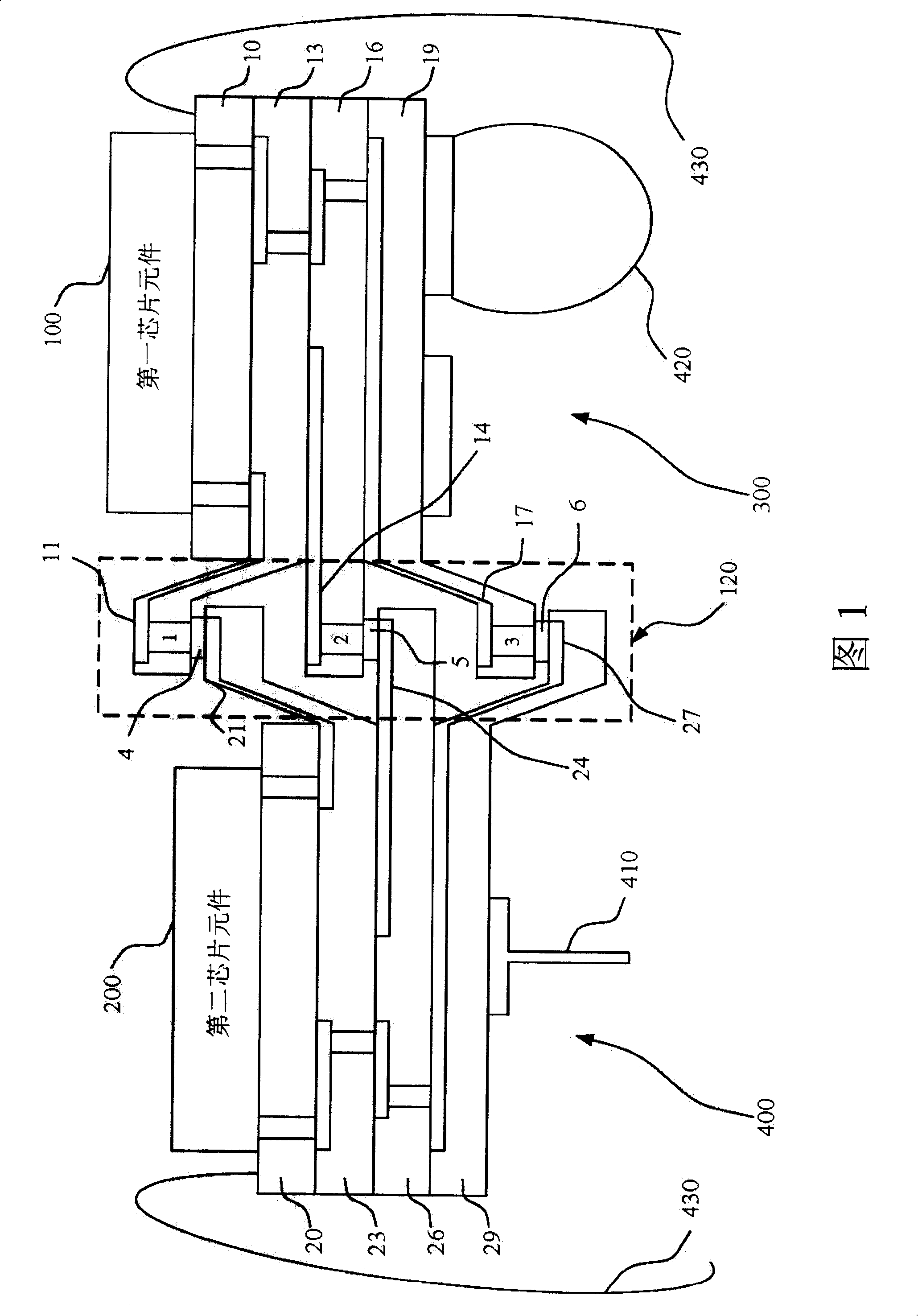
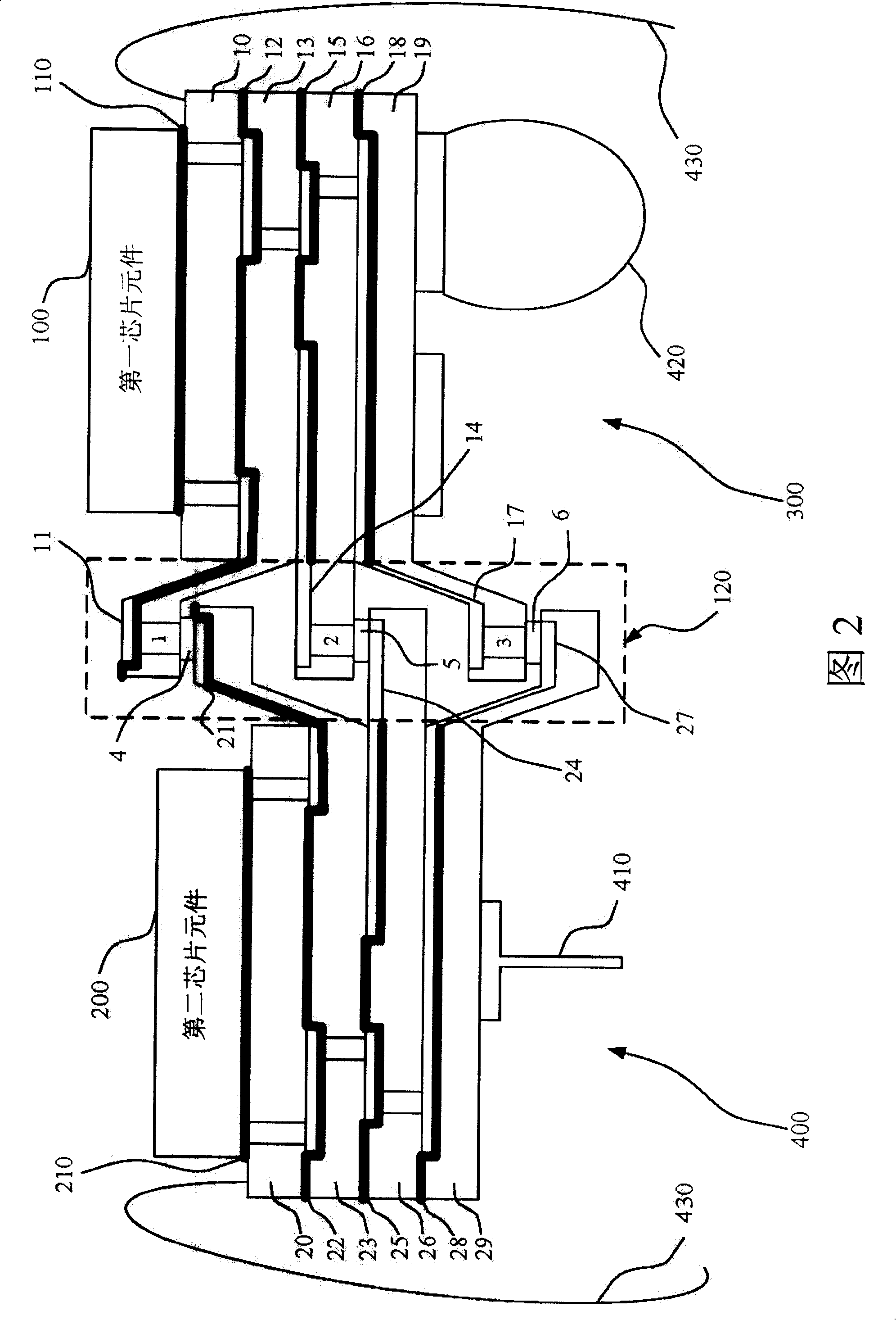
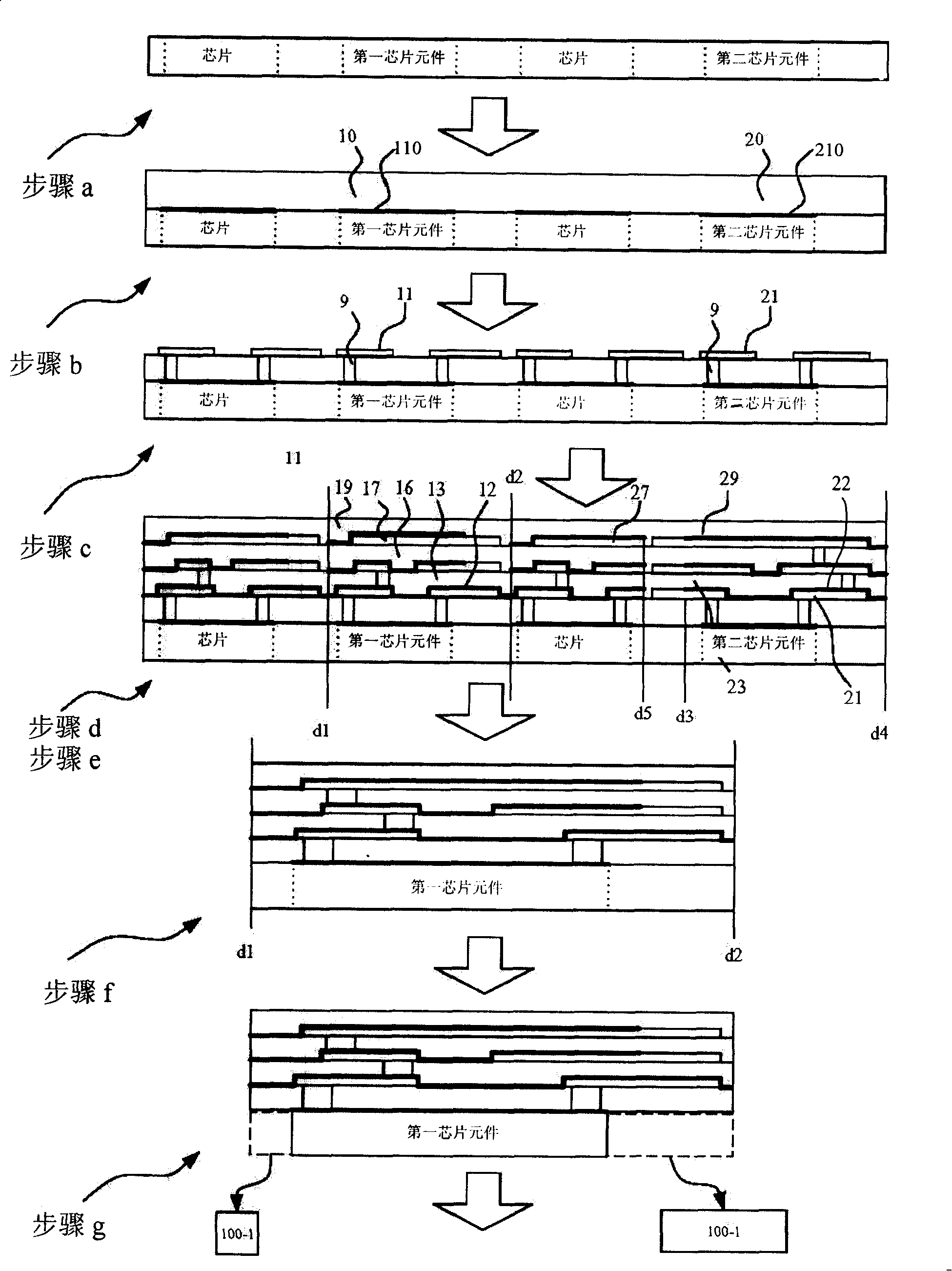
[0026] Please refer to FIG. 1 , which is a cross-sectional view of an interconnection structure between multilayer substrates according to an embodiment of the present invention. The interconnection structure between multilayer substrates at least includes a first multilayer substrate 300 , a second multilayer substrate 400 and a plurality of via holes 1 , 2 and 3 formed on the first multilayer substrate 300 . The first outer surface of the first multilayer substrate 300 is connected to a first chip component 100 , and the first outer surface of the second multilayer substrate 400 is connected to a second chip component 200 . The first chip component 100 and the second chip component 200 may be any type of chip components such as logic components, memory components, analog components, optoelectronic components, micro-electrome...
PUM
 Abstract
Description
Claims
Application Information