Integrated SiCr metal thin film resistors for SiGe RF-BiCMOS technology

A technology of metal thin film resistors and thin film resistors, which is applied in the manufacture of circuits, electrical components, semiconductors/solid-state devices, etc., can solve problems such as the limitation of thin film resistance values, achieve the effects of reducing parasitic effects and increasing packaging density

Inactive Publication Date: 2007-08-29
NXP BV
View PDF0 Cites 3 Cited by
  • Summary
  • Abstract
  • Description
  • Claims
  • Application Information

AI Technical Summary

Problems solved by technology

However, materials commonly used to produce integrated metal thin film resistors such as TaN, NiCr and TaSi

Method used


Image

  • Integrated SiCr metal thin film resistors for SiGe RF-BiCMOS technology
  • Integrated SiCr metal thin film resistors for SiGe RF-BiCMOS technology
  • Integrated SiCr metal thin film resistors for SiGe RF-BiCMOS technology

Examples


Embodiment Construction

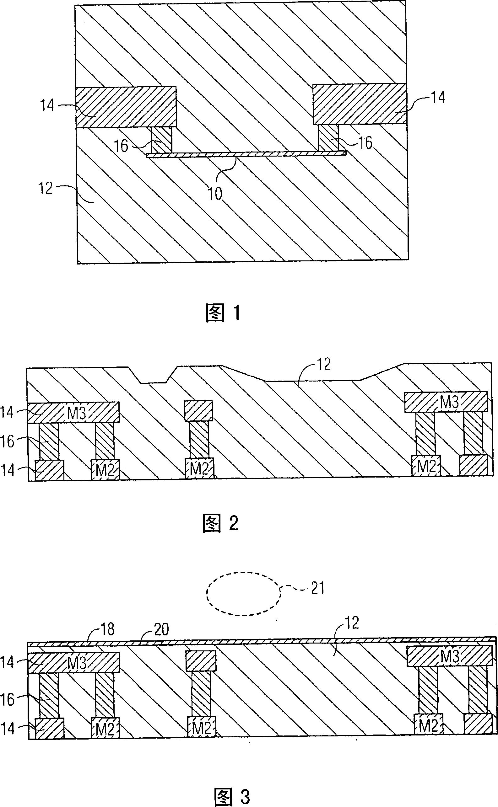
[0021] Referring to FIG. 1 , there is shown a SEM (scanning electron microscope) cross-sectional view of a SiCr metal thin film resistor 10 produced according to an embodiment of the present invention. For example, in silicon dioxide (SiO 2 ) form a SiCr thin film resistor 10 on a high-density planarized dielectric substrate 12 . SiCr thin film resistor 10 is directly connected to upper metal level 14 via via 16 .

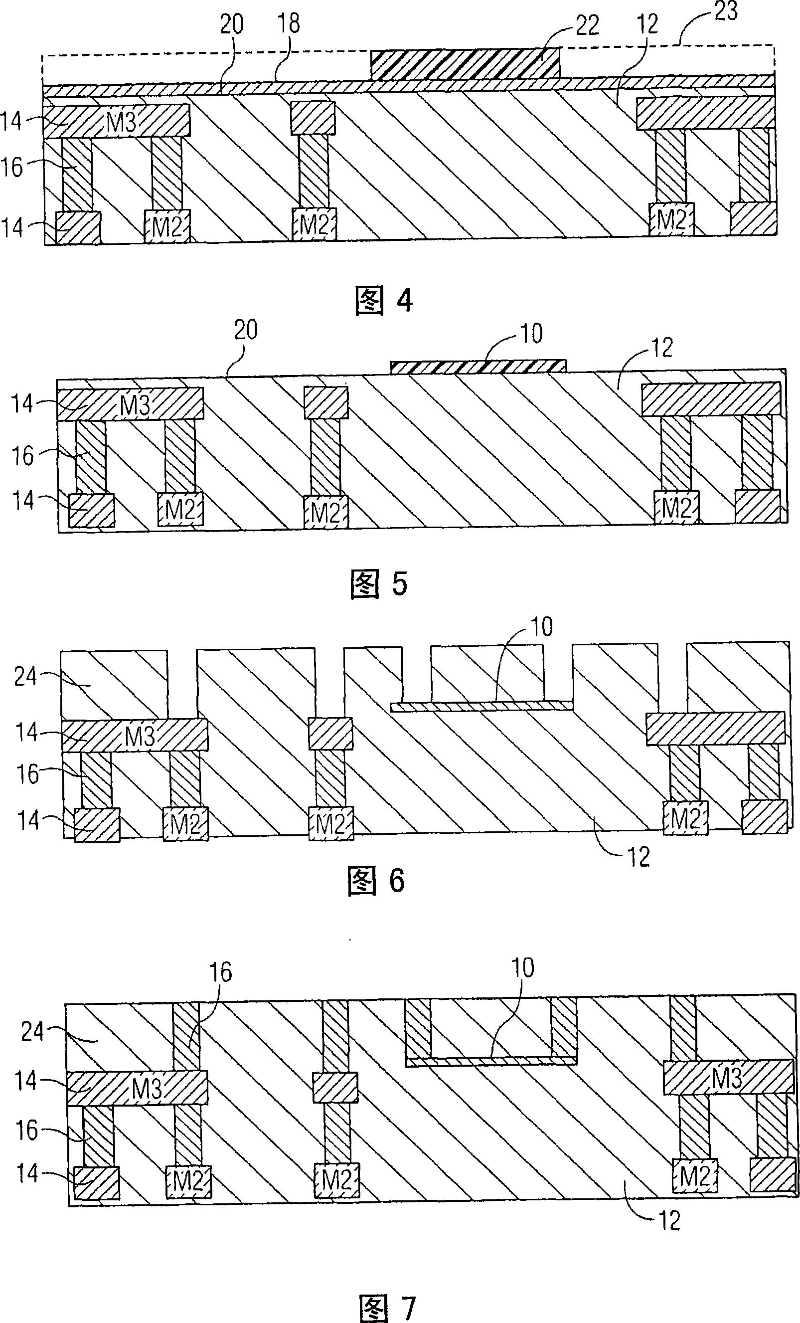
[0022] Referring to FIGS. 2 to 8 , a method for forming a SiCr thin film resistor 10 according to an embodiment of the present invention is shown.

[0023] In FIG. 2 , a high density dielectric substrate 12 is shown comprising a plurality of metal layers 14 (eg, M2 , M3 ) interconnected by vias 16 . Metal layer 14 and vias 16 are formed using conventional photolithographic techniques. For example, dielectric substrate 12 may be formed using a high density plasma (HDP) chemical vapor deposition (CVD) process. For example, other suitable techniques including plas...


PUM


Abstract

The present invention provides integrated SiCr metal thin film resistors (10) for SiGe RF BiCMOS technology. The use of integrated SiCr thin film resistors (10) increases packaging density and reduces the parasitic effect induced from surface mount configurations at high frequencies. In accordance with the present invention, the sheet resistance (Rs) of SiCr thin film resistors can be varied in a wide range of about 400 - 2500 ohms/square with less than 2% uniformity by selectively controlling SiCr deposition conditions. In addition, SiCr thin film resistors formed in accordance with the present invention have linear and quadratic coefficients of TCR less than about 100 ppml DEG C and -0.9 ppm/ DEG C2, respectively.

Description

technical field [0001] The present invention generally relates to semiconductor devices. More specifically, the present invention relates to the formation of integrated SiCr metal thin film resistors for SiGeRF-BiCMOS (Radio Frequency Bipolar Complementary Metal Oxide Semiconductor) technology. Background technique [0002] The advent of wireless communication and the corresponding beginning growth of high-frequency use in millimeter wave fashion has brought new demands not only for enhanced performance but also for reduced package and module size at the same time. These demands require highly integrated packages and modules for high frequency applications. [0003] The use of integrated passive components such as thin film resistors significantly reduces surface mount parasitics at high frequencies, increases packaging density, and improves manufacturability. This drives the need for improvements in the RF and analog performance of passive components required for system-l...

Claims


Application Information

Patent Timeline
IPC IPC(8): H01L21/02
Inventor 红江·孙卡曼·鲁佩吉·麦克唐纳南希·E·贝尔塔伊尔·纳什瓦特
Owner NXP BV
Why Eureka
Try Eureka