Integrated COBLED (Chip on Board Light-emitting Diode) encapsulation structure

A technology of integrated packaging and installation grooves, applied in the field of lighting, can solve the problems of poor light-emitting effect, poor air-tightness, and poor heat-dissipation effect, so as to improve LED life and stability, improve light-emitting rate, and ensure air-tightness and physical strength Effect

Inactive Publication Date: 2012-01-18
ZHEJIANG INTELED OPTOELECTRONICS TECH
View PDF5 Cites 2 Cited by
  • Summary
  • Abstract
  • Description
  • Claims
  • Application Information

AI Technical Summary

Problems solved by technology

[0003] The present invention mainly solves the technical problems of poor heat dissipation effect, light output effect and poor air tightness existing in the int

Method used


Image

  • Integrated COBLED (Chip on Board Light-emitting Diode) encapsulation structure
  • Integrated COBLED (Chip on Board Light-emitting Diode) encapsulation structure
  • Integrated COBLED (Chip on Board Light-emitting Diode) encapsulation structure

Examples


Example Embodiment

[0016] Examples:

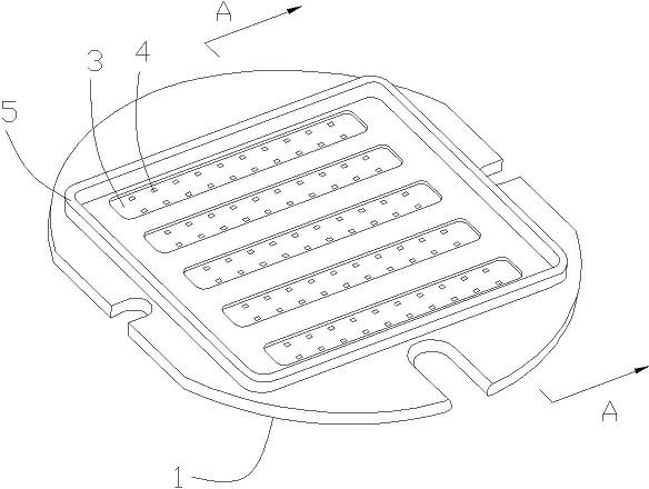
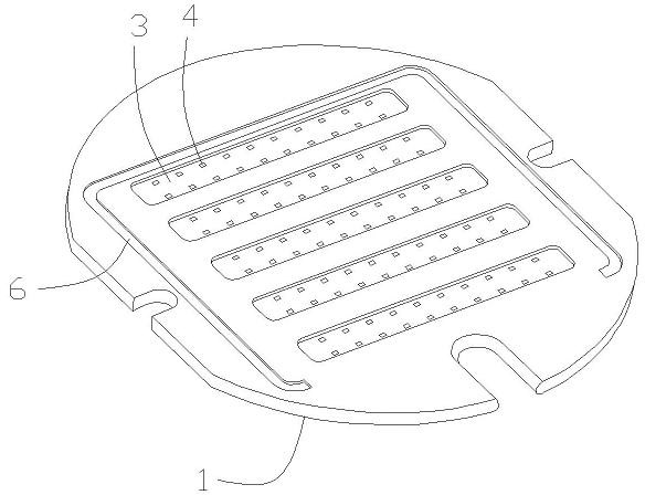
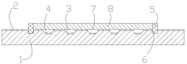
[0017] In this embodiment, a COBLED integrated packaging structure, such as figure 1 with image 3 As shown, it includes a substrate 1 and a circuit layer 2 arranged on the surface of the substrate. The substrate is an aluminum substrate. There are five parallel strip grooves 3 arranged on the substrate. In this embodiment, the light-emitting chip 4 emits blue light. The light-emitting chips are evenly arranged at the bottom of the strip groove 3, and the light-emitting chips are connected to the circuit layer 2 on the substrate through wire bonding, such as image 3 As shown, the side wall of the strip groove is inclined, forming a reflector structure. Such as figure 2 As shown, an installation groove 6 is provided on the periphery of the strip groove. The installation groove surrounds the strip groove on three sides. There is also a ring of wall glue 5 on the periphery of the strip groove. The wall glue surrounds the strip groove and the bottom of the wall ...


PUM


Abstract

The invention relates to an integrated COBLED (Chip on Board Light-emitting Diode) encapsulation structure, which solves the technical problems of poor radiation effect, bad emergent light effect and air tightness in the existing integrated COBLED encapsulation structure. A COBLED comprises a substrate and a circuit layer arranged on the substrate, a plurality of strip-shaped slots which are arranged in parallel are arranged on the substrate, luminous chips are evenly distributed at the bottom of the strip-shaped slots, a circle of enclosure glue is arranged at the peripheries of the strip-shaped slots, and transparent glue is filled in a region surrounded by the enclosure glue. The integrated COBLED encapsulation structure has the advantages that the luminous chips are integrated in the strip-shaped slots so as to improve the encapsulation density of the luminous chips, and the luminous chips are directly contacted with the substrate, thus having a good radiation effect; the luminous chips can conduct radiation through the substrate, and current passes through the circuit layer on the surface of the substrate, thus forming a heat-electricity separation structure and further increasing the service life and stability of an LED (light-emitting diode); and the enclosure glue is embedded in the substrate, thus ensuring the air tightness and physical strength of the encapsulation; and the side walls of the strip-shaped slots are oblique, thus improving the light extraction rate of the luminous chips.

Description

technical field [0001] The invention relates to the technical field of lighting, in particular to a COBLED integrated packaging structure with good heat dissipation, light emission and sealing effects. Background technique [0002] The existing COBLED (Chip on Board) generally arranges the light-emitting chip on the circuit layer on the surface of the substrate, and forms a potting area of ​​glue by pressing a circle of plastic compound on the periphery, or makes a lead frame on the surface of the substrate to fill the wall glue , or press a layer of glue on the substrate, make a tapered hole in the glue, arrange the LED chip in the tapered hole and seal it with glue. However, these packaging solutions also have many disadvantages. For example, the light-emitting chip is not in direct contact with the substrate, but passes through a circuit layer with extremely low thermal conductivity. The overall heat dissipation effect is very poor. Not good, the pressed plastic packagin...

Claims


Application Information

Patent Timeline
IPC IPC(8): H01L25/075H01L33/48H01L33/64H01L33/62H01L33/52
Inventor 陈华
Owner ZHEJIANG INTELED OPTOELECTRONICS TECH
Why Eureka
Try Eureka