Method of manufacturing semiconductor device having transition metal oxide layer and related device

a technology of transition metal oxide layer and semiconductor device, which is applied in the direction of semiconductor device, digital storage, instruments, etc., can solve problems such as memory cell malfunction

Active Publication Date: 2009-01-22
SAMSUNG ELECTRONICS CO LTD
View PDF4 Cites 45 Cited by
  • Summary
  • Abstract
  • Description
  • Claims
  • Application Information

AI Technical Summary

Problems solved by technology

A snake current can cause memory cells to malfunction.

Method used


Image

  • Method of manufacturing semiconductor device having transition metal oxide layer and related device
  • Method of manufacturing semiconductor device having transition metal oxide layer and related device
  • Method of manufacturing semiconductor device having transition metal oxide layer and related device

Examples


experimental examples

[0110]FIG. 14 is a graph showing the characteristics of a varistor manufactured according to exemplary embodiments of the present invention.

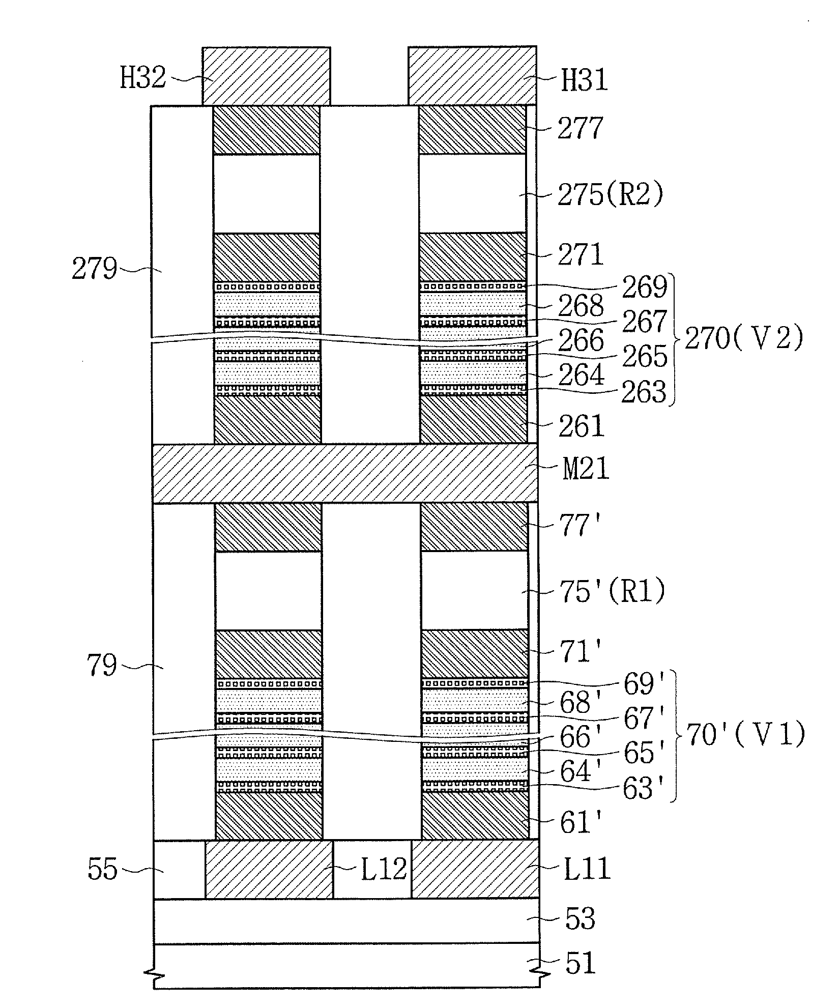
[0111]In FIG. 14, a voltage applied to both ends of the varistor is plotted on the horizontal axis, the unit is volt (V), a current flowing through the varistor is plotted on the vertical axis, and the unit is ampere (A). The varistor was formed to include first and second electrodes, first to tenth transition metal oxide patterns and first to tenth leakage control patterns. The first and second electrodes were formed of an Ir layer, each of the transition metal oxide patterns was formed of a TiO layer, to which Ir was added, to have a thickness of 1.5 nm, and each of the leakage control patterns was formed of a Mg layer of a thickness of 0.5 nm.

[0112]Curve 142 of FIG. 14 shows current-voltage characteristics of the varistor. As shown by curve 142, the varistor exhibited current characteristics close to 0 within a bias interval from −0.5V to +0....


PUM


Abstract

Provided is a method of manufacturing a semiconductor device having a switching device capable of preventing a snake current. First, a transition metal oxide layer and a leakage control layer are alternately stacked on a substrate 1 to 20 times to form a varistor layer. The transition metal oxide layer is formed to contain an excessive transition metal compared to its stable state. The leakage control layer may be formed of one selected from the group consisting of a Mg layer, a Ta layer, an Al layer, a Zr layer, a Hf layer, a polysilicon layer, a conductive carbon group layer, and a Nb layer.

Description

CROSS-REFERENCE TO RELATED APPLICATION[0001]This application claims the benefit of Korean Patent Application No. 10-2007-0072959, filed Jul. 20, 2007, the contents of which are hereby incorporated herein by reference in their entirety.BACKGROUND OF THE INVENTION[0002]1. Field of the Invention[0003]The present invention relates generally to semiconductor memory devices and, more particularly, to methods of manufacturing semiconductor devices.[0004]2. Description of the Related Art[0005]Research into high integration of memory devices has been widespread. A memory device includes a plurality of word lines, a plurality of bit lines, and a plurality of memory cells. Memory devices are classified as volatile memory devices and non-volatile memory devices depending on characteristics of data stored in the memory cells. A non-volatile memory device maintains data stored in the memory cells even when power is cut off.[0006]A non-volatile memory device includes a flash memory, a Magnetic Ran...

Claims


Application Information

Patent Timeline
Patent Type & Authority Applications(United States)
IPC IPC(8): H01L21/329H01L47/00
CPCG11C13/003H01L27/24H01L27/224G11C2213/76H10B61/10H10B63/00H10B63/80
Inventor JEONG, JUN-HOLEE, JANG-EUNOH, SE-CHUNGNAM, KYUNG-TAEBAEK, IN-GYU
Owner SAMSUNG ELECTRONICS CO LTD
Why Eureka
Try Eureka