Time-interleaved analog-to-digital-converter

a converter and time-interleave technology, applied in the field of time-interleaved analog-to-digital converters, can solve the problems of increasing the circuit area and power consumption of the ti-adc, adding an undesired portion to the circuit area and the effect of reducing the influence of offset errors

Inactive Publication Date: 2009-01-22
CSR TECH INC
View PDF15 Cites 16 Cited by
  • Summary
  • Abstract
  • Description
  • Claims
  • Application Information

AI Technical Summary

Benefits of technology

[0006]It is an object of the present invention to provide a TI-ADC with reduced susceptibility to o...

Problems solved by technology

Offset errors in the sub ADCs contribute to distortion, such as spurious tones, in the output of the TI-ADC.
Such compensation requires DSP circuitry, which ad...

Method used


Image

  • Time-interleaved analog-to-digital-converter
  • Time-interleaved analog-to-digital-converter
  • Time-interleaved analog-to-digital-converter

Examples


Embodiment Construction

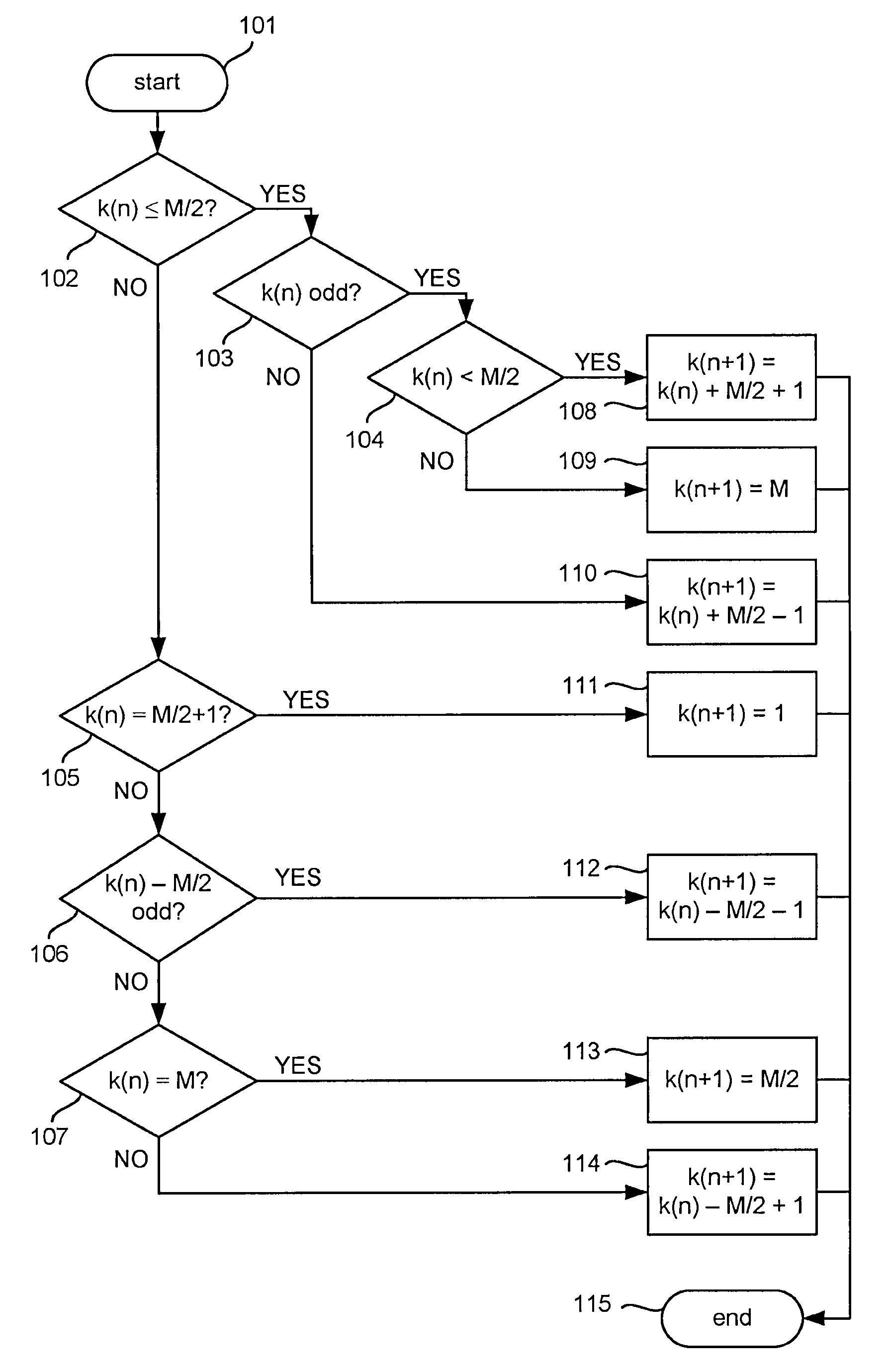
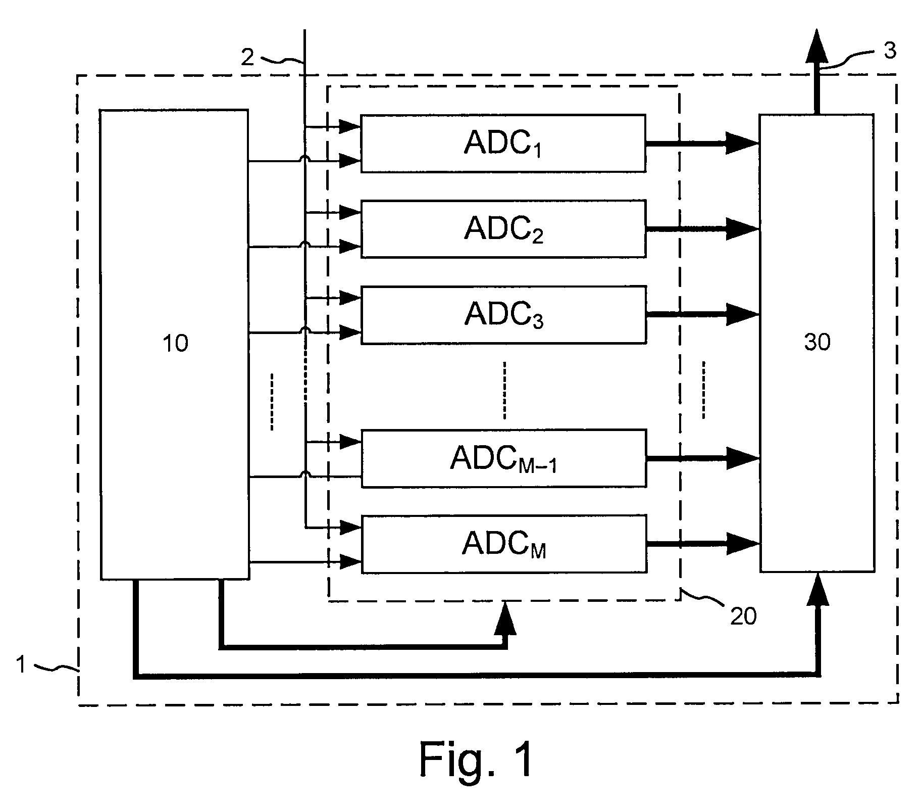
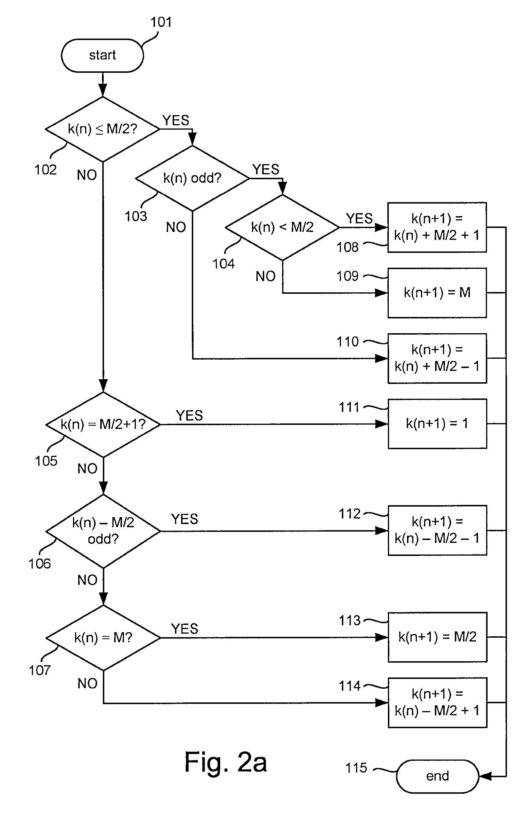
[0063]FIG. 1 shows a block diagram of a time-interleaved (TI) analog-to-digital converter (ADC) 1 according to an embodiment. The TI-ADC 1 may comprise an array 20 of M sub ADCs ADC1, . . . , ADCM, where M may be an even integer. Each row of the array 20 may comprise exactly one of the sub ADCs ADC1, . . . , ADCM, as indicated in FIG. 1. The placement of sub ADCs in FIG. 1 reflects the physical placement of sub ADCs on a chip or integrated circuit, i.e. ADC1 may be placed in a first row of the array, ADC2 may be placed in a second row adjacent to the first row, etc., and ADCM may be placed in a last row of the array. Each of the sub ADCs ADC1, . . . , ADCM operate at a common first clock frequency or sampling frequency. Sampling instants of the sub ADCs ADC1, . . . , ADCM are mutually displaced in time, so as to achieve effective sampling of the TI-ADC 1 at a second clock frequency or sampling frequency, which is higher than the first clock frequency or sampling frequency with a fac...


PUM


Abstract

A method for operating a time-interleaved analog-to-digital converter for converting an analog input to a digital output using a time-interleaved analog-to-digital converter, wherein the time-interleaved analog-to-digital converter comprises an array of M sub ADCs (ADC1, ADC2, . . . , ADCM), where M is an even integer, and each row of the array comprises one of the M sub ADCs. The method comprises the step of, for every sampling instant n, where n is an integer in a sequence of integers, converting the analog input by means of the sub ADC in row k(n) of the array, wherein 1≦k(n)≦M. A value between 1 and M is assigned to k(n) for the first sample instant, and k(n+1) is selected such that a) k(n+1)>M/2 if k(n)≦M/2, otherwise k(n+1)≦M/2; b) M/2−1≦|k(n+1)−k(n)|≦M/2+1; and c) k(n+1)=k(m+1) if and only if n−m is an integer multiple of M. A time interleaved analog-to-digital converter operating in accordance with the method is also disclosed.

Description

TECHNICAL FIELD OF THE INVENTION[0001]The present invention relates to a time-interleaved analog-to-digital converter. It also relates to a method for controlling the time-interleaved analog-to-digital converter.[0002]Description of Related Art[0003]A time-interleaved (TI) analog-to-digital converter (ADC) utilizes a plurality of sub ADCs with a common analog input. The plurality of sub ADCs operate at a common first clock frequency or sampling frequency. A multi-phase clock unit is used to generate individual clock signals for each sub ADC. The individual clock signals generated by the multi-phase clock unit are mutually displaced in time, so as to achieve effective sampling for the TI-ADC at a second clock frequency or sampling frequency which is higher than the first clock frequency or sampling frequency with a factor equal to the number of sub ADCs in the TI-ADC.[0004]The sub ADCs in a TI-ADC are normally operated in an order corresponding to their physical placement on a chip. ...

Claims


Application Information

Patent Timeline
IPC IPC(8): H03M1/12
CPCH03M1/1215H03M1/1205H03M1/12
Inventor GUSTAFSSON, STAFFAN
Owner CSR TECH INC
Why Eureka
Try Eureka