High profile minimum contact process kit for hdp-cvd application

a technology of hdpcvd and process kit, which is applied in the direction of liquid surface applicators, coatings, chemical vapor deposition coatings, etc., can solve the problem that the features of the top and bottom surfaces are not parallel with each other

Inactive Publication Date: 2009-01-29
APPLIED MATERIALS INC
View PDF10 Cites 14 Cited by
  • Summary
  • Abstract
  • Description
  • Claims
  • Application Information

AI Technical Summary

Benefits of technology

[0008]A wafer processing system is also disclosed according to another embodiment of the invention. The wafer processing system may include a housing defining a process chamber, a high-density plasma generating system operatively coupled to the process chamber, a gas-delivery system configured to introduce gases into the process chamber, a pressure-control system for maintaining a selected pressure within the process chamber, and a wafer support member as described above.

Problems solved by technology

However, some features of the top and bottom surfaces might not be parallel with each other.

Method used


Image

  • High profile minimum contact process kit for hdp-cvd application
  • High profile minimum contact process kit for hdp-cvd application
  • High profile minimum contact process kit for hdp-cvd application

Examples


Embodiment Construction

[0019]The ensuing description provides preferred exemplary embodiment(s) only, and is not intended to limit the scope, applicability or configuration of the disclosure. Rather, the ensuing description of the preferred exemplary embodiment(s) will provide those skilled in the art with an enabling description for implementing with an exemplary embodiment. It should be understood that various changes may be made in the function and arrangement of elements without departing from the spirit and scope as set forth in the appended claims.

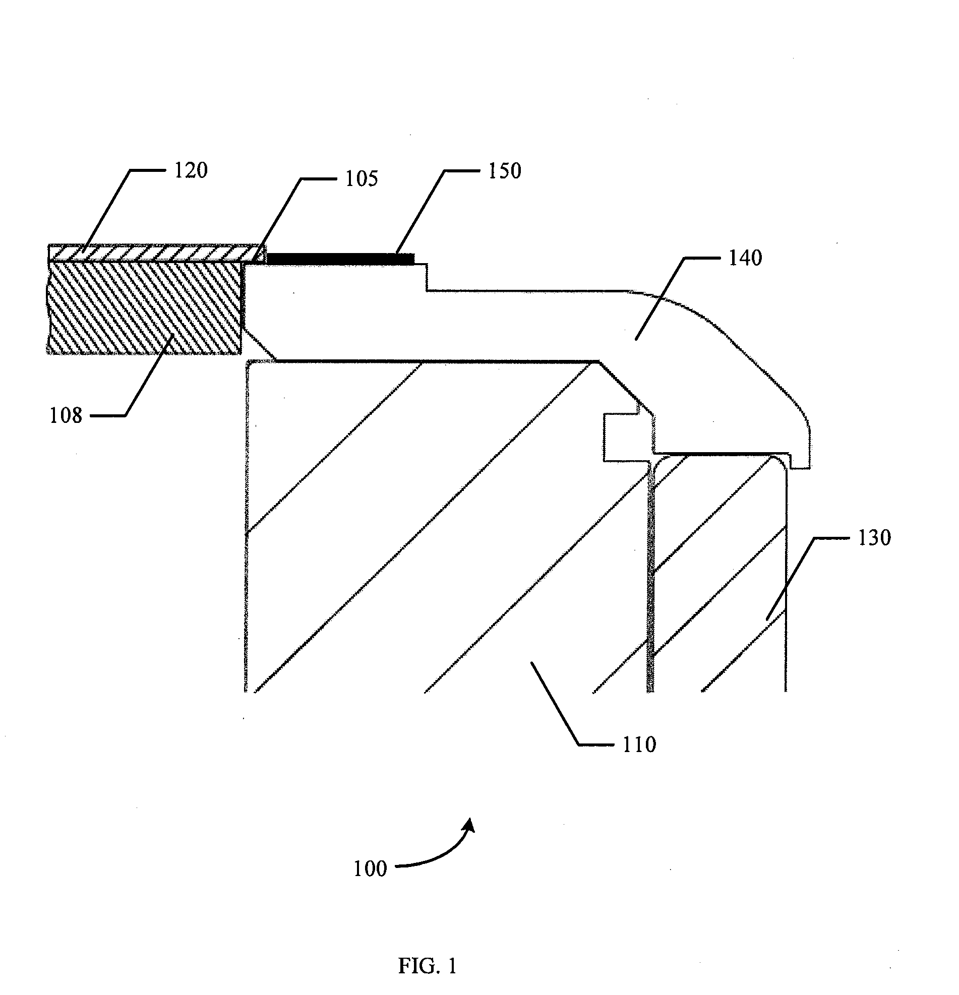
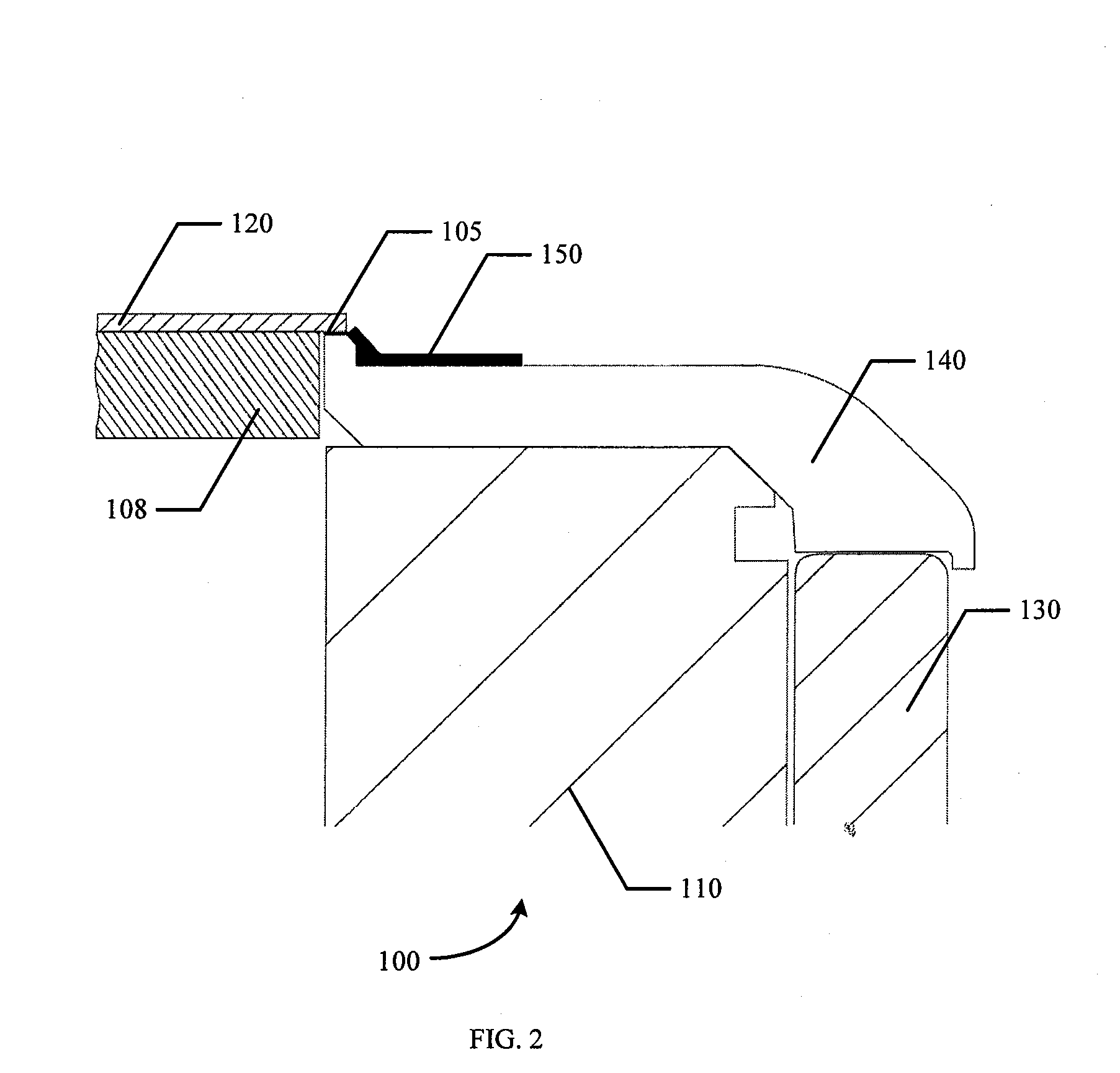
[0020]In one embodiment, the present disclosure provides for a CVD process kit cover with a high profile feature. The process kit cover may be a generally circular ring-shaped structure. The high profile feature may be disposed over the process kit cover near a wafer facing surface. The wafer facing surface is disposed over the interior edge of the process kit cover. The high profile feature substantially surrounds a wafer when the wafer is placed on the w...


PUM

PropertyMeasurementUnit
thickaaaaaaaaaa
temperatureaaaaaaaaaa

Abstract

A process kit cover for chemical vapor deposition processes is disclosed according to one embodiment of the invention. The process kit cover may include a protrusion from the top surface of the process kit cover. The protrusion is adjacent to a wafer facing surface. The protrusion decreases oxide buildup on the process kit cover and the wafer facing surface during repeated deposition processes. The process kit cover may also be in minimal thermal contact at the interface with a lower support structure, such as a ceramic collar or pedestal, according to another embodiment of the invention. Minimal thermal contact may be achieved by placing an insulator between the process kit cover and the lower support structure or by creating a gap or gaps between the process kit cover and the lower support structure. Ambient atmosphere may provide thermal insulating within the gap or gaps.

Description

BACKGROUND OF THE INVENTION[0001]One of the primary steps in the fabrication of modern semiconductor devices is the formation of a thin film on a semiconductor wafer by chemical reaction of gases. Such a deposition process is referred to as chemical vapor deposition (“CVD”). Conventional thermal CVD processes supply reactive gases to the wafer surface where heat-induced chemical reactions take place to produce a desired film. Plasma-enhanced CVD (“PECVD”) techniques, on the other hand, promote excitation and / or dissociation of the reactant gases by the application of radio-frequency (“RF”) energy to a reaction zone near the wafer surface, thereby creating a plasma. The high reactivity of the species in the plasma reduces the energy required for a chemical reaction to take place and, thus, lowers the temperature required for such CVD processes as compared to conventional thermal CVD processes. These advantages are further exploited by high-density-plasma (“HDP”) CVD techniques, in wh...

Claims


Application Information

Patent Timeline
Patent Type & Authority Applications(United States)
IPC IPC(8): H01L21/683
CPCH01L21/68721C23C16/4585
Inventor RASHEED, MUHAMMAD
Owner APPLIED MATERIALS INC
Why Eureka
Try Eureka