Method and apparatus for cleaning a substrate surface

a technology of substrate surface and cleaning method, which is applied in the direction of chemically reactive gas, crystal growth process, epitaxial silicon layer, etc., can solve the problems of high energy consumption, wafer to wafer variation in wafer lots, and the surface of monocrystalline silicon and epitaxial silicon is susceptible to contamination, etc., and achieves low energy consumption.

Active Publication Date: 2009-01-29
APPLIED MATERIALS INC
View PDF24 Cites 409 Cited by
  • Summary
  • Abstract
  • Description
  • Claims
  • Application Information

AI Technical Summary

Problems solved by technology

Surfaces of the monocrystalline silicon and the epitaxial silicon layer are susceptible to contamination when exposed to typical ambient conditions.
However, wet cleaning processes have “queue time” issues, which can cause wafer to wafer variation in wafer lots due to varying idle times for different wafers in a lot.
Conventional remote or in-situ plasma cleaning processes can be very challenging due to the contamination of the chamber and substrates processed in the chamber due to the creation of unwanted species that are formed in the gas phase or during the cleaning process.
These unwanted species either limit the cleaning action of the desired species or introduce other complications to the cleaning process.

Method used


Image

  • Method and apparatus for cleaning a substrate surface
  • Method and apparatus for cleaning a substrate surface
  • Method and apparatus for cleaning a substrate surface

Examples


Embodiment Construction

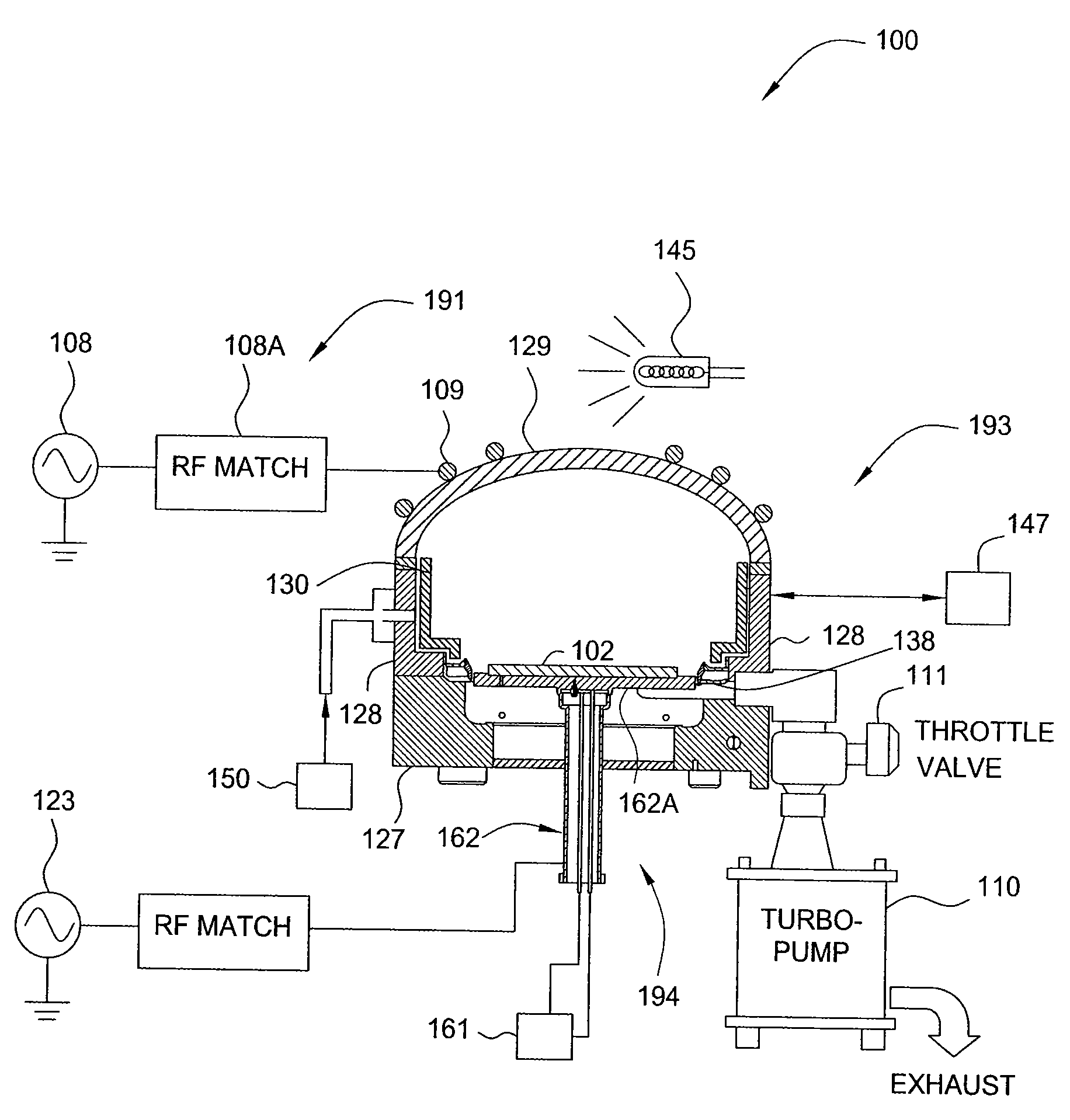
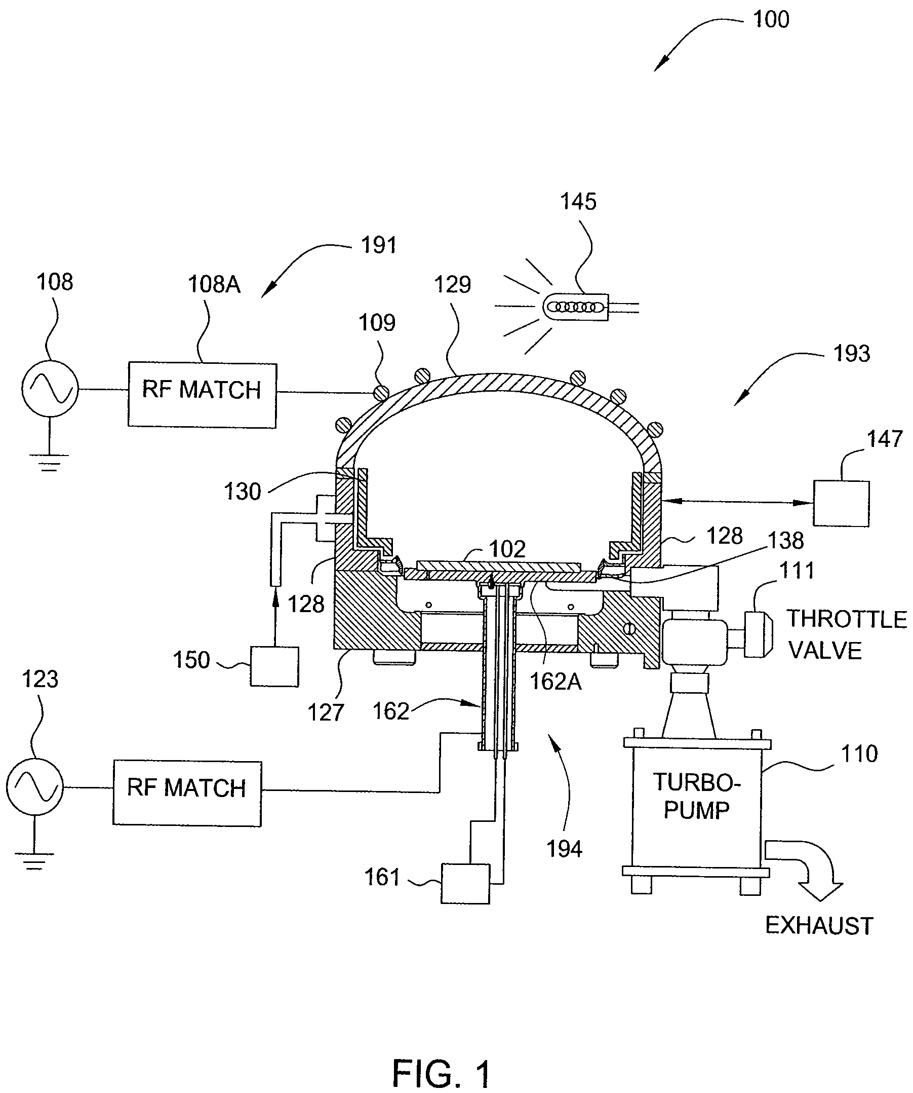
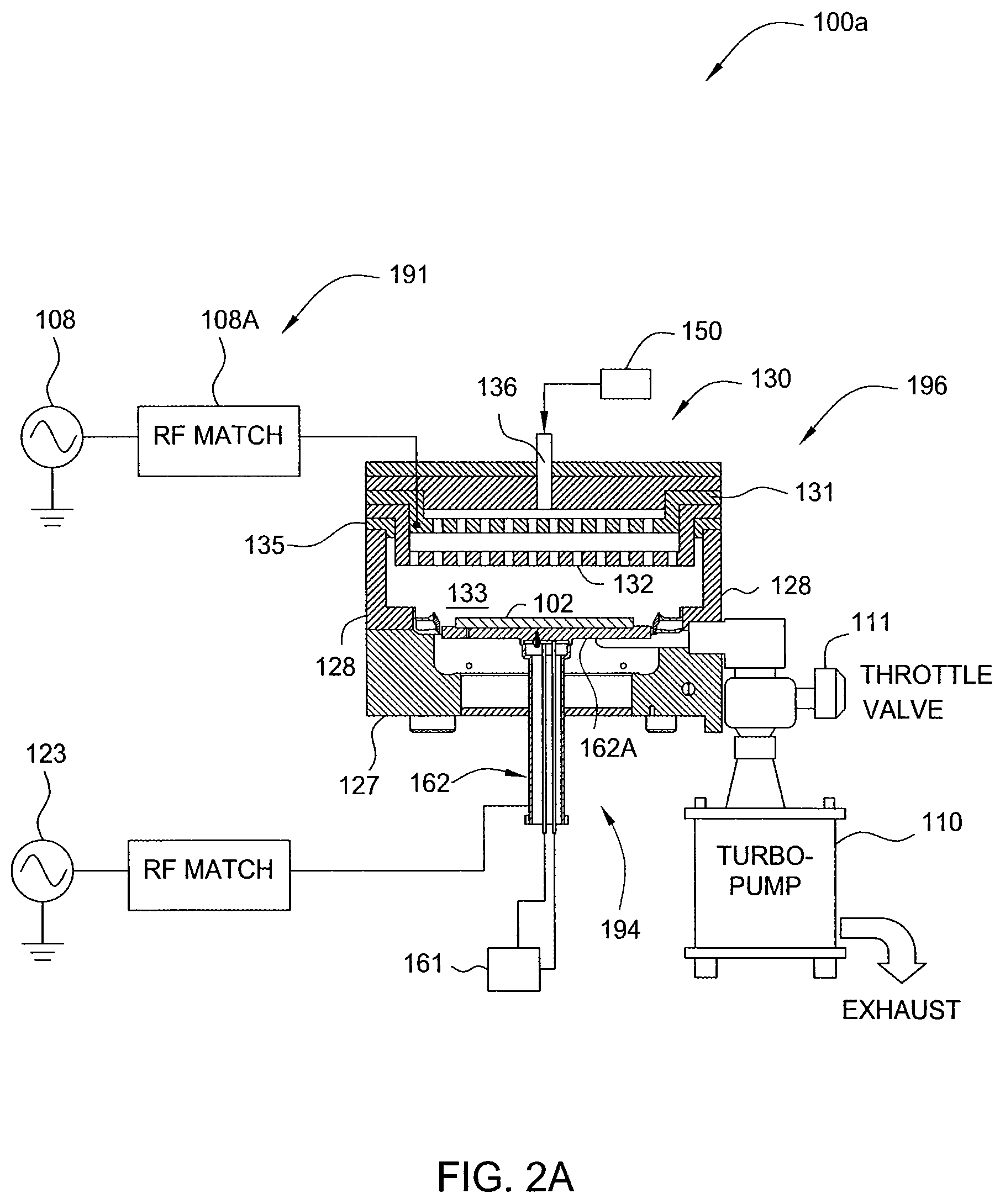
[0021]The present invention generally provides apparatus and method for forming a clean and damage free surface on a semiconductor substrate (or wafer). One embodiment of the present invention provides a system that contains a cleaning chamber that is adapted to expose a surface of substrate to a plasma cleaning process prior to forming an epitaxial layer thereon. In one embodiment, a method is employed to reduce the contamination of a substrate processed in the cleaning chamber by depositing a gettering material on the inner surfaces of the cleaning chamber prior to performing a cleaning process on a substrate. The gettering material will tend to trap contaminants found in the cleaning chamber, thus insuring that the processed substrate is clean, and future substrates processed in the chamber will have the same desirable cleaning results. In one embodiment, oxidation and etching steps are repeatedly performed on a substrate in the cleaning chamber to expose or create a clean surfac...


PUM

PropertyMeasurementUnit
RF poweraaaaaaaaaa
temperatureaaaaaaaaaa

Abstract

The present invention generally provides apparatus and method for forming a clean and damage free surface on a semiconductor substrate. One embodiment of the present invention provides a system that contains a cleaning chamber that is adapted to expose a surface of substrate to a plasma cleaning process prior to forming an epitaxial layer thereon. In one embodiment, a method is employed to reduce the contamination of a substrate processed in the cleaning chamber by depositing a gettering material on the inner surfaces of the cleaning chamber prior to performing a cleaning process on a substrate. In one embodiment, oxidation and etching steps are repeatedly performed on a substrate in the cleaning chamber to expose or create a clean surface on a substrate that can then have an epitaxial placed thereon. In one embodiment, a low energy plasma is used during the cleaning step.

Description

CROSS-REFERENCE TO RELATED APPLICATIONS[0001]This application claims the benefit of the U.S. Provisional Patent Application Ser. No. 60 / 952,230 [Attorney Docket No. 12588L], filed Jul. 26, 2007, which is herein incorporated by reference.BACKGROUND OF THE INVENTION[0002]1. Field of the Invention[0003]Embodiments of the present invention generally relate to method and apparatus for processing a semiconductor substrate. More particularly, embodiments of the present invention relate to method and apparatus for cleaning a surface of a silicon substrate.[0004]2. Description of the Related Art[0005]Integrated circuits are formed in and on silicon and other semiconductor substrates. In the case of single crystal silicon, substrates are made by growing an ingot from a bath of molten silicon, and then sawing the solidified ingot into multiple wafers. An epitaxial silicon layer may then be formed on the monocrystalline silicon wafer to form a defect free silicon layer that may be doped or undo...

Claims


Application Information

Patent Timeline
Patent Type & Authority Applications(United States)
IPC IPC(8): H01L21/322C23F1/08H01L21/20
CPCC30B25/08H01L21/67017H01L21/67069H01L21/02238H01L21/0262H01L21/31662H01L21/02046Y10S438/976H01L21/67028H01L21/02255H01L21/02532H01L21/02661C30B29/06H01L21/20
Inventor SANCHEZ, ERROL ANTONIO C.SWENBERG, JOHANESCARLSON, DAVID K.DOHERTY, ROISIN L.
Owner APPLIED MATERIALS INC
Why Eureka
Try Eureka