Cleaning process for microelectronic dielectric and metal structures

a technology of metal structure and cleaning process, which is applied in the direction of basic electric elements, electrical equipment, semiconductor/solid-state device manufacturing, etc., can solve the problems of ineffective or ineffective cleaning of microelectronics

Inactive Publication Date: 2009-01-29
IBM CORP
View PDF14 Cites 10 Cited by
  • Summary
  • Abstract
  • Description
  • Claims
  • Application Information

AI Technical Summary

Benefits of technology

[0015]In a first instance, the invention provides a plurality of methods for cleaning a dielectric and metal structure within a microelectronic structure. A first particular method includes: (1) an oxygen plasma treatment of the dielectric and metal structure; followed by (2) an alcohol treatment of the dielectric and metal structure; followed by; (3) an aqueous organic acid treatment of the dielectric and metal structure. A second method includes: (1) an aqueous surfactant treatment of the dielectric and metal structure; followed by (2) an alcohol treatment of the dielectric and metal structure; followed by; (3) an aqueous organic acid treatment of the dielectric and metal structure. The first method is useful in cleaning a plasma etch residue from the dielectric and metal structure, which preferably comprises a dual damascene aperture. The second method is useful in cleaning a chemical mechanical polish planarizing residue from the dielectric and metal structure, which preferably comprises a contiguous via and interconnect layer located and planarized within the dual damascene aperture to provide a dual damascene structure.

Problems solved by technology

While effective and efficient cleaning processes are certainly desirable at any stage of microelectronic structure fabrication, effective and efficient cleaning processes are often particularly desirable within the context of microelectronic dielectric and metal structure fabrication, since ineffectively or inefficiently cleaned microelectronic dielectric and metal structures are often readily discernible through electrical measurements.

Method used


Image

  • Cleaning process for microelectronic dielectric and metal structures
  • Cleaning process for microelectronic dielectric and metal structures
  • Cleaning process for microelectronic dielectric and metal structures

Examples


Embodiment Construction

[0021]The invention, which provides: (1) a plurality of methods for cleaning a dielectric and metal structure within a microelectronic structure; as well as (2) a method for fabricating a dual damascene structure within a microelectronic structure, is understood within the context of the description set forth below. The description set forth below is understood within the context of the drawings described above. Since the drawings are intended for illustrative purposes, the drawings are not necessarily drawn to scale.

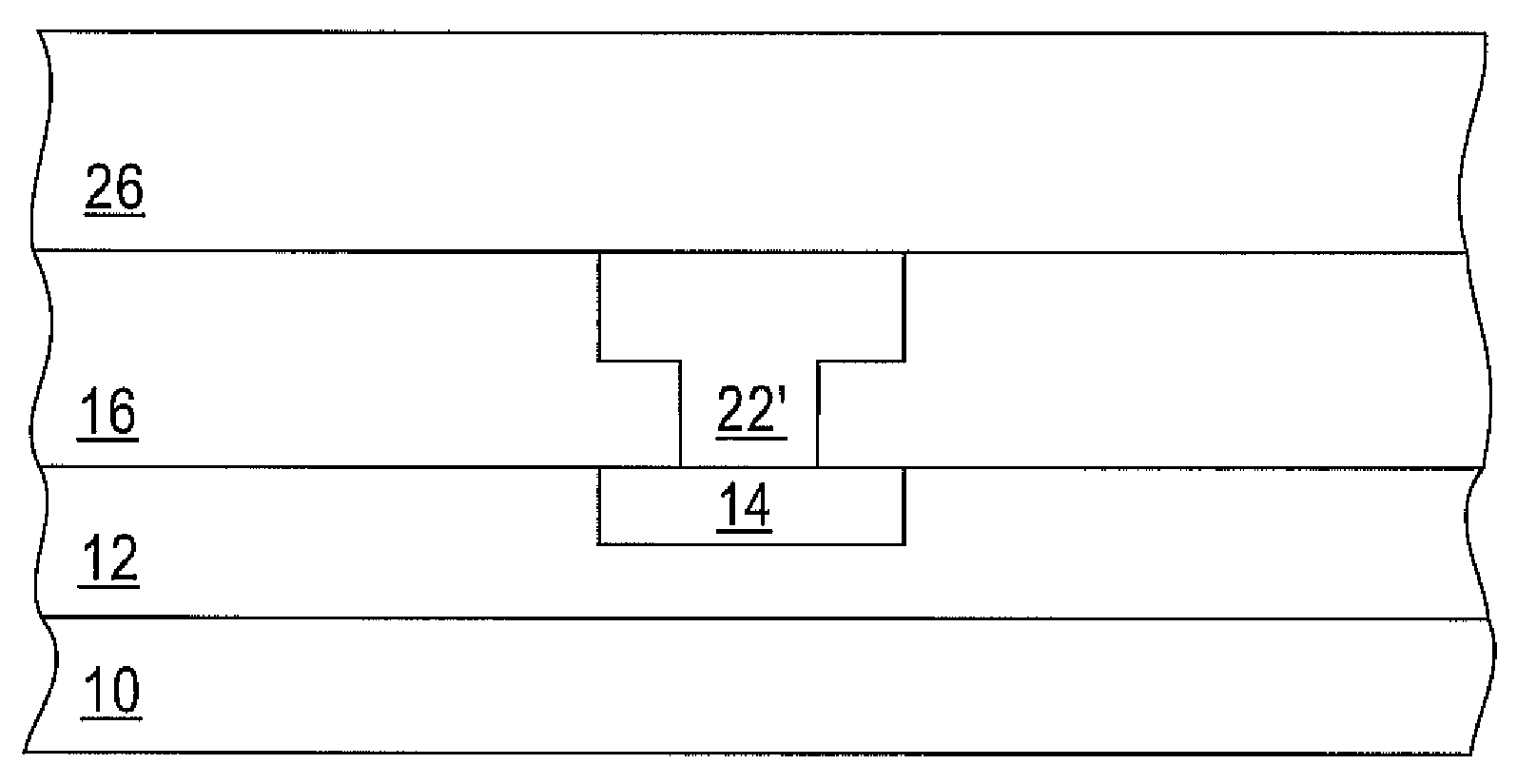
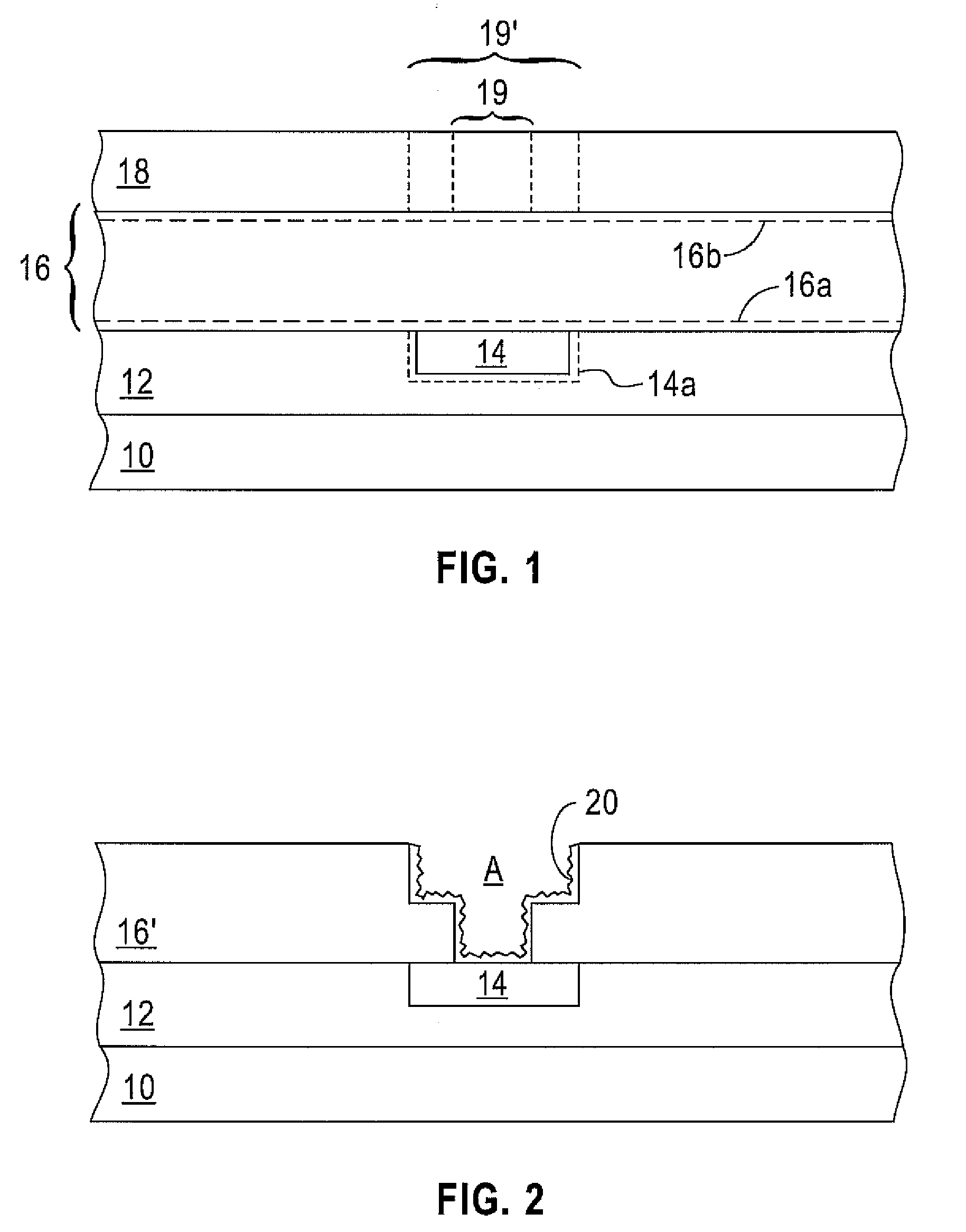
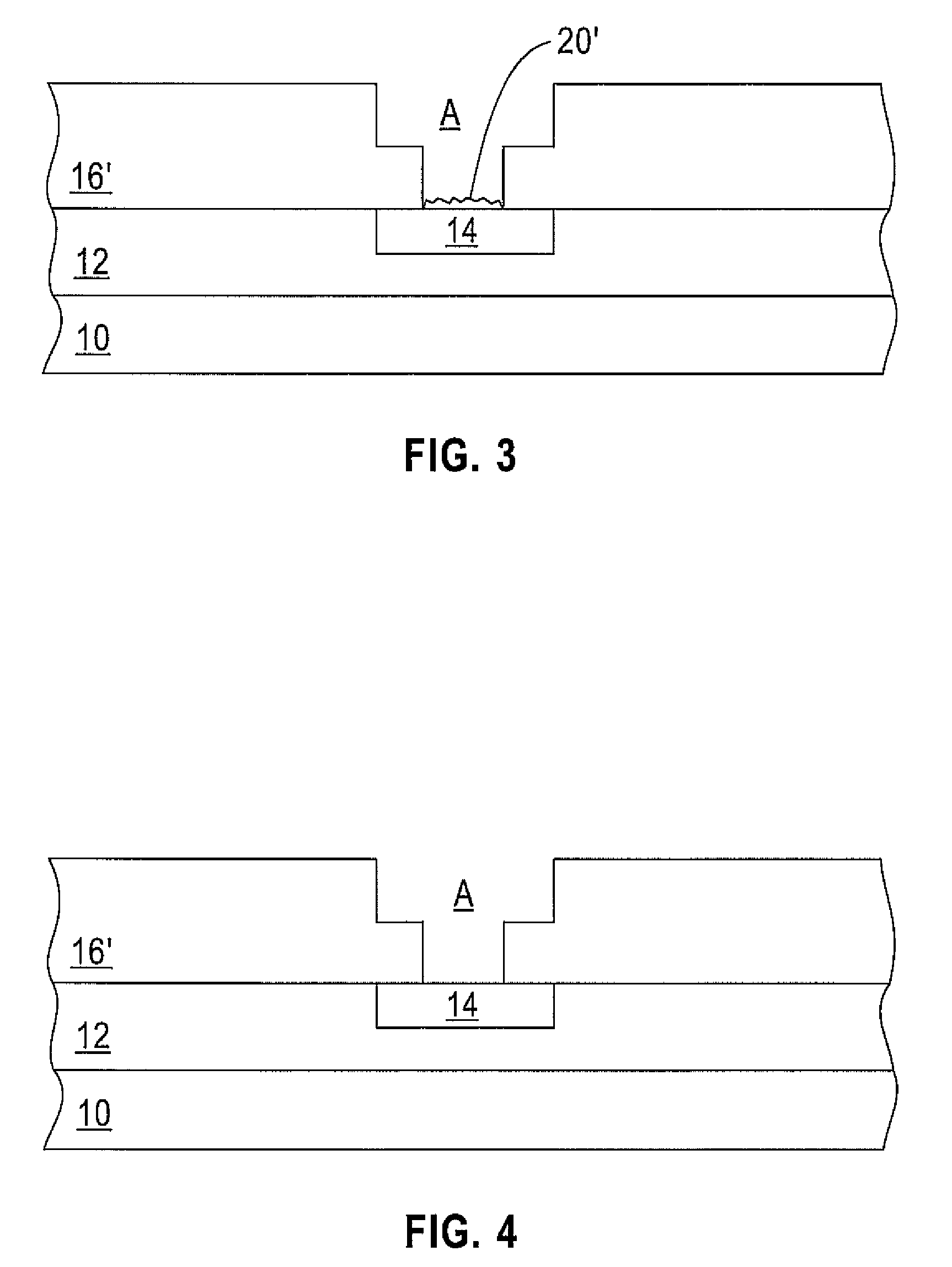
[0022]FIG. 1 to FIG. 10 shows a series of schematic cross-sectional diagrams illustrating the results of progressive stages in fabricating a semiconductor structure in accordance with a particular embodiment of the invention. This particular embodiment of the invention comprises a preferred embodiment of the invention.

[0023]While the preferred embodiment illustrates the invention within the context of a semiconductor structure, neither the embodiment, nor the invention,...


PUM


Abstract

A method for cleaning a dielectric and metal structure within a microelectronic structure uses an oxygen containing plasma treatment, followed by an alcohol treatment, in turn followed by an aqueous organic acid treatment. Another method for cleaning a dielectric and metal structure within a microelectronic structure uses an aqueous surfactant treatment followed by an alcohol treatment and finally followed by an aqueous organic acid treatment. The former method may be used to clean a plasma etch residue from a dual damascene aperture. The second method may be used to clean a chemical mechanical polish planarizing residue from a dual damascene structure. The two methods may be used sequentially, absent any intervening or subsequent sputtering method, to provide a dual damascene structure within a microelectronic structure.

Description

BACKGROUND[0001]1. Field of the Invention[0002]The invention relates generally to cleaning processes for microelectronic structures. More particularly, the invention relates to cleaning processes for microelectronic dielectric and metal structures.[0003]2. Description of the Related Art[0004]Microelectronic structures, and in particular semiconductor structures, are generally fabricated using successive layering processes that are intended to fabricate successive portions of a microelectronic structure over a microelectronic substrate, such as a semiconductor substrate. The fabrication of successive portions of a microelectronic structure over a microelectronic substrate may use any of several microelectronic fabrication processes. Non-limiting examples include ion implant processes, photolithographic processes, selective etch processes and selective deposition processes.[0005]Common in the microelectronic fabrication art is the use of cleaning processes for cleaning microelectronic...

Claims


Application Information

Patent Timeline
Patent Type & Authority Applications(United States)
IPC IPC(8): H01L21/768
CPCH01L21/02063H01L21/76814H01L21/02074
Inventor ROTHWELL, MARY BETHYU, ROY RONGQING
Owner IBM CORP
Why Eureka
Try Eureka