Method of manufacturing semiconductor device

a manufacturing method and semiconductor technology, applied in semiconductor/solid-state device manufacturing, basic electric elements, electric devices, etc., can solve the problems of degrading em characteristic of the upper wiring and cannot meet the demand, and achieve the effect of reducing the roughness of the surface, enhancing em resistance, and reducing the resistance of vias

Inactive Publication Date: 2009-01-29
PANASONIC CORP
View PDF7 Cites 1 Cited by
  • Summary
  • Abstract
  • Description
  • Claims
  • Application Information

AI Technical Summary

Benefits of technology

[0038]Thus, with the barrier metal film remaining on the bottom surface of the trench, the metal barrier film can be removed from the bottom surface of the via, and the lower wiring exposed from the bottom surface of the via can be engraved. Therefore, via resistance can be reduced without degrading the EM resistance of the upper wiring.
[0039]Furthermore, the lower wiring exposed from the bottom surface of the via is modified, and the modified layer is removed to form the recess portion (engraving) in the lower wiring. This enables a reduction in the roughness of a surface of the lower wiring (a surface of the recess portion) exposed from the bottom surface of the via. Thus, the via plug and the lower wiring can be more tightly contacted with each other, allowing the EM resistance to be enhanced.
[0040]Furthermore, after the formation of the via and the trench, during the deposition of the barrier metal film over the via and the trench, the barrier metal film deposition rate ratio of the bottom surface of the trench to the bottom surface of the via is set higher than the barrier metal removal rate ratio of the bottom surface of the trench to the bottom surface of the via. Consequently, the barrier metal can be reliably left on the bottom surface of the trench.
[0041]Furthermore, first, the trench is formed, and the barrier metal film is then deposited over the trench. Then, the via is formed, and the barrier metal film is deposited again. Consequently, the barrier metal can be reliably left on the bottom surface of the trench.
[0042]As described above, the method of manufacturing a semiconductor device according to the present invention can reduce the via resistance and is thus useful for miniaturized and integrated semiconductor devices.

Problems solved by technology

However, the demand cannot be met simply by removing the barrier metal film from the bottom surface of the via.
Thus, disadvantageously, the EM characteristic of the upper wiring is degraded.

Method used


Image

  • Method of manufacturing semiconductor device
  • Method of manufacturing semiconductor device
  • Method of manufacturing semiconductor device

Examples


embodiment 1

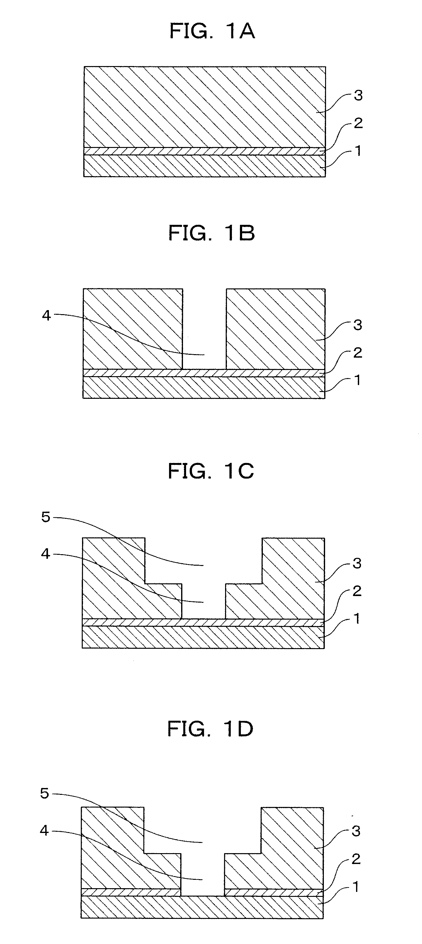
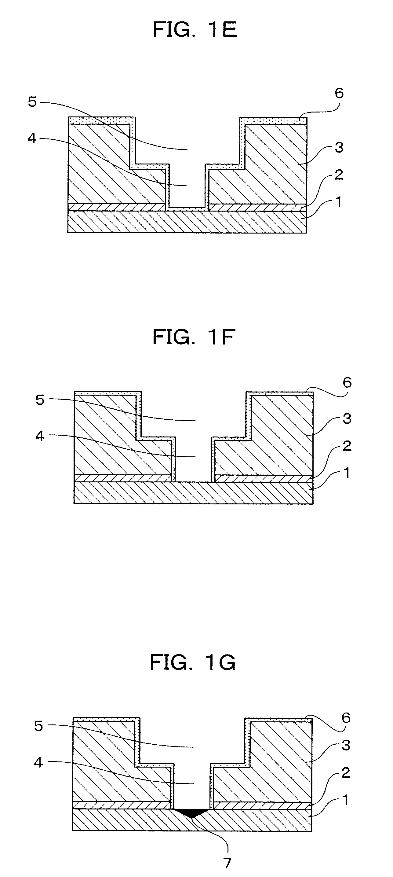
[0064]A method of manufacturing a semiconductor device according to Embodiment 1 of the present invention will be described below with reference to FIGS. 1A to 1J. FIGS. 1A to 1J are sectional views showing steps of the method of manufacturing the semiconductor device according to Embodiment 1 of the present invention.

[0065]First, as shown in FIG. 1A, lower wiring 1 is formed on a semiconductor substrate with an element such as a transistor formed thereon. Then, an insulating barrier film 2 is formed on the lower wiring 1 by a CVD method. SiCO or SiCN is used as the insulating barrier film 2. Subsequently, an interlayer insulating film 3 is formed on the insulating barrier film 2 by a CVD method. A carbon-containing silicon oxide film (SiOC film) is used as the interlayer insulating film 3.

[0066]Then, as shown in FIG. 1B, a photo resist having a via pattern is deposited on the interlayer insulating film 3 by a photolithography method. The interlayer insulating film 3 is subsequently...

embodiment 2

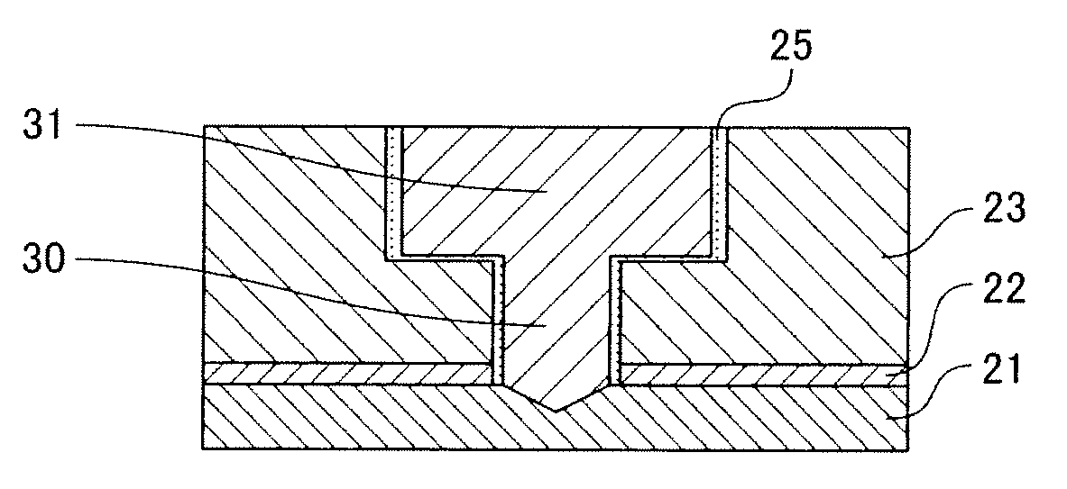
[0083]A method of manufacturing a semiconductor device according to Embodiment 2 of the present invention will be described below with reference to FIGS. 2A to 2J. FIGS. 2A to 2J are sectional views showing steps of the method of manufacturing the semiconductor device according to Embodiment 2 of the present invention.

[0084]First, as shown in FIG. 2A, lower wiring 21 is formed on a semiconductor substrate with an element such as a transistor formed thereon. Then, an insulating barrier film 22 is formed on the lower wiring 21 by a CVD method. SiCO or SiCN is used as the insulating barrier film 22. Subsequently, an interlayer insulating film 23 is formed on the insulating barrier film 22 by a CVD method. A carbon-containing silicon oxide film (SiOC film) is used as the interlayer insulating film 23.

[0085]Then, as shown in FIG. 2B, a photo resist having a trench pattern is deposited on the interlayer insulating film 23 by a photolithography method. The interlayer insulating film 23 is ...


PUM

PropertyMeasurementUnit
thicknessaaaaaaaaaa
bias poweraaaaaaaaaa

Abstract

The present invention provides a method of manufacturing a semiconductor device which method enables a reduction in via resistance. The method of manufacturing the semiconductor device includes the steps of removing a barrier metal film from a bottom surface of a via, with the barrier metal film remaining on a bottom surface of a trench, modifying lower wiring exposed from the bottom surface of the via to form a modified layer, removing the modified layer to form an engraving (recess portion), and depositing a copper film in the engraving, the via, and the trench to form upper wiring and a via plug.

Description

FIELD OF THE INVENTION[0001]The present invention relates to a method of manufacturing a semiconductor device having wiring formed by a dual damascene method.BACKGROUND OF THE INVENTION[0002]Most recent semiconductor integrated circuits have wiring of a multilayer structure in order to deal with the increased degree of integration and a reduced chip size. Furthermore, an increasing number of recent semiconductor integrated circuits use copper (Cu) wiring in order to prevent a possible delay in signal propagation.[0003]A dual damascene method is a technique for forming such Cu wiring of a multilayer structure. The dual damascene method will be described in brief. First, an insulating film is formed on lower wiring. A wiring groove (trench) for upper wiring and a connection hole (via) for a via plug are formed on the insulating film: the connection hole connects the upper wiring and the lower wiring together. A barrier metal film is subsequently formed on a bottom surface and side sur...

Claims


Application Information

Patent Timeline
Patent Type & Authority Applications(United States)
IPC IPC(8): H01L21/768
CPCH01L21/2855H01L21/76805H01L21/76807H01L21/76888H01L21/76835H01L21/76844H01L21/76834
Inventor TORAZAWA, NAOKI
Owner PANASONIC CORP
Why Eureka
Try Eureka