Conducting wire and contact opening forming method for reducing photoresist thickness and via resistance

a technology of contact opening and conducting wire, which is applied in the direction of basic electric elements, electrical equipment, semiconductor devices, etc., can solve the problems of reducing the accuracy of the etched profile, affecting the effect of etching accuracy, and affecting the etching quality of the remaining metal portions, so as to reduce the required thickness of photoresist

Active Publication Date: 2005-12-27
NAN YA TECH
View PDF6 Cites 0 Cited by
  • Summary
  • Abstract
  • Description
  • Claims
  • Application Information

AI Technical Summary

Benefits of technology

[0014]An objective of the present invention is to provide a method for forming conducting wire and contact opening in semiconductor structure, which can reduces the required thickness of photoresist used in the process.
[0015]Another objective of the present invention is to provide a method for forming conducting wire and contact opening in semiconductor structure, by which the via resistance can be reduced.

Problems solved by technology

If the photoresist portion inclines or collapses, the accuracy of the etched profile is degraded, causing the pattern consisting of the remaining metal portions after etching is different from the predetermined pattern.
However, in the etching process, the protective layer 164 of the conducting wire corresponding to the contact opening 175 is often undesirably etched off, resulting in the damage to the conducting wire, and causing the via resistance increases.

Method used


Image

  • Conducting wire and contact opening forming method for reducing photoresist thickness and via resistance
  • Conducting wire and contact opening forming method for reducing photoresist thickness and via resistance
  • Conducting wire and contact opening forming method for reducing photoresist thickness and via resistance

Examples


Embodiment Construction

[0022]An embodiment of the present invention will be described in detail with reference to the accompanying drawings.

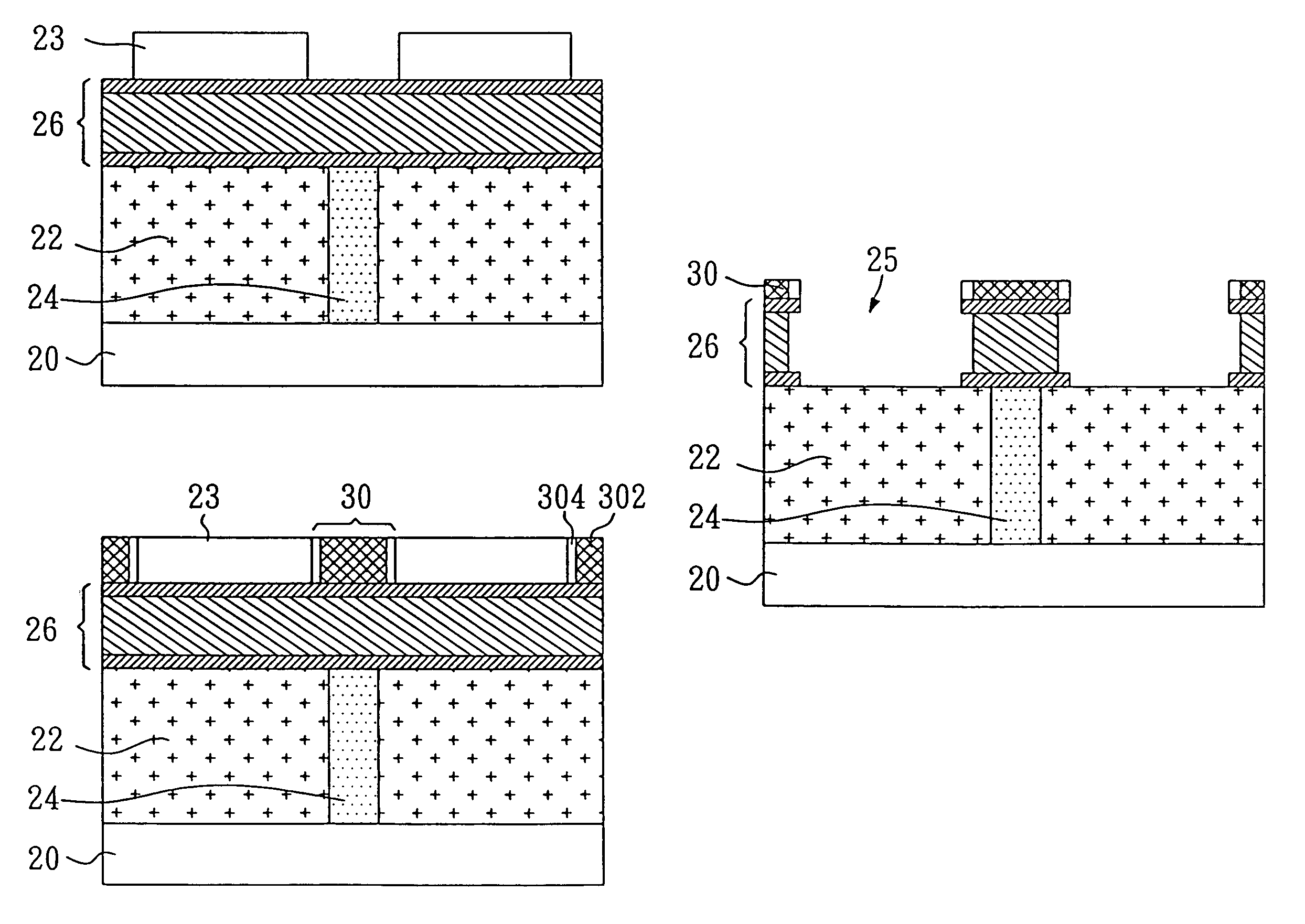
[0023]The structures shown in FIGS. 2a and 2b are the same as those shown in FIGS. 1a and 1b, and therefore the descriptions thereof are omitted herein. In the drawings, reference number 20 indicates a substrate, 22 indicates a first dielectric layer, 24 indicates a via filled with metal, 26 indicates a conductive layer, which includes a metal layer 260 of aluminum, and protective layers 262 and 264 formed on the top and bottom of the metal layer 260. The material of the protective layers can be Ti / TiN.

[0024]A second dielectric layer 23, of which the material can be oxide, preferably NSG (non-doped silicon glass), is formed on the conductive layer 26, as shown in FIG. 2c. Then, a photoresist layer 28 of a predetermined pattern is formed on the second dielectric layer 23 to define the position where a contact opening is to be formed, as shown in FIG. 2d. The portions o...


PUM


Abstract

Disclosed is a method for forming conducting wire and contact opening in a semiconductor device. The method of the present invention utilizes the formation of metal regions as a mask for etching a conductive layer of the semiconductor device to remove unnecessary portions so as to form conducting wires. The method of the present invention can reduce the necessary thickness of photoresist and well control the via resistance.

Description

BACKGROUND OF THE INVENTION[0001]1. Field of the Invention[0002]The present invention relates to a process for conducting wire and contact opening in semiconductor structure, more specifically, to a method for reducing photoresist thickness and via resistance in conducting wire process.[0003]2. Description of the Prior Art[0004]In manufacturing semiconductor devices such as DRAM, the process for forming conducting wires is very important.[0005]A conventional process for forming conducting wires will be described with reference to FIG. 1.[0006]First, a first dielectric layer 12 is formed on a semiconductor substrate 10. The first dielectric layer 12 is dug to form a via 14, and the via 14 is filled with metal. The resultant structure is shown in FIG. 1a. [0007]Then, on the first dielectric layer 12 comprising the via 14 filled with metal, a conductive layer 16 is formed. In practical process, the conductive layer 16 comprises a metal layer 160 of aluminum, aluminum / copper or any othe...

Claims


Application Information

Patent Timeline
Patent Type & Authority Patents(United States)
IPC IPC(8): H01L21/3213H01L21/4763H01L21/768
CPCH01L21/32139H01L21/76838H01L21/7685H01L21/76865H01L2221/1078
Inventor HUANG, TSE-YAOCHEN, YI-NANSHIH, CHIANG-LIN
Owner NAN YA TECH
Why Eureka
Try Eureka