Trench gate field effect transistor with charge balance structure and manufacturing method thereof

A field-effect transistor and charge balancing technology, which is applied in semiconductor/solid-state device manufacturing, circuits, electrical components, etc., can solve the problem of large occupied area

Active Publication Date: 2021-09-14
济南安海半导体有限公司
View PDF4 Cites 0 Cited by
  • Summary
  • Abstract
  • Description
  • Claims
  • Application Information

AI Technical Summary

Problems solved by technology

[0002] With the rapid development of electronic information technology, especially the rapid development of fashion consumer electronics and portable products, the demand for power devices such as metal oxide semiconductor field effect transistors (MOSFETs) is increasing. MOSFETs are mainly divided into horizontal and vertical Two, the obvious advantage of the lateral MOSFET is its better integration, which can be more easily integrated into the process platform of the existing technology, but because its withstand voltage drift region is spread out on the surface, it shows its biggest shortcoming, occupying The larger the area, the area represents the cost, and the higher the withstand voltage, the more obvious the disadvantage

Method used


Image

  • Trench gate field effect transistor with charge balance structure and manufacturing method thereof
  • Trench gate field effect transistor with charge balance structure and manufacturing method thereof
  • Trench gate field effect transistor with charge balance structure and manufacturing method thereof

Examples


Embodiment Construction

[0050] In order to understand the technical content of the present invention more clearly, the following examples are given in detail.

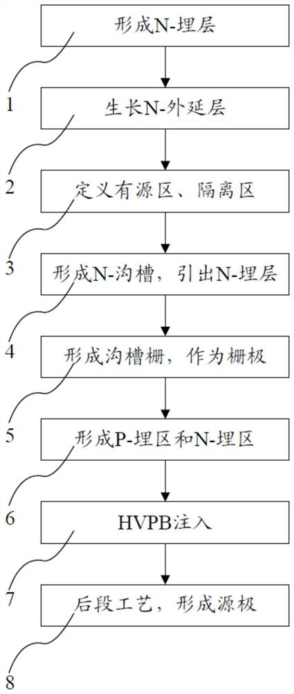
[0051] see figure 2 Shown is a flow chart of the steps of the manufacturing method of the trench gate field effect transistor with the charge balance structure of the present invention.

[0052] In one embodiment, the manufacturing method of the trench gate field effect transistor with charge balance structure includes the following steps:

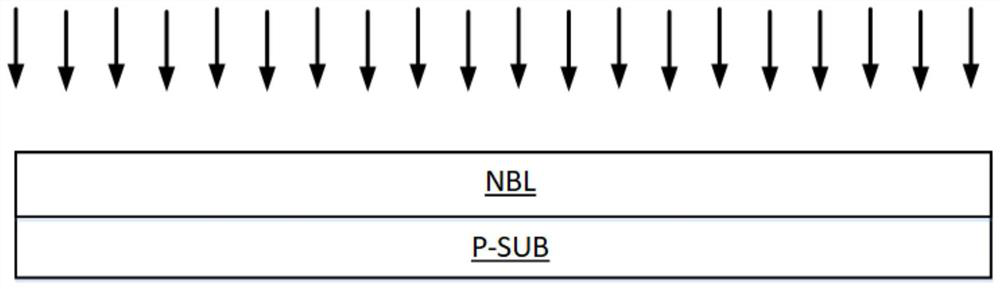
[0053] (1) if image 3 As shown, phosphorus is implanted on the P-substrate to form an N-buried layer;

[0054] (2) if Figure 4 As shown, an N-epitaxial layer is grown on the N-buried layer;

[0055] (3) if Figure 5 As shown, an active region is defined above the top of the device and two isolation regions are placed within the device;

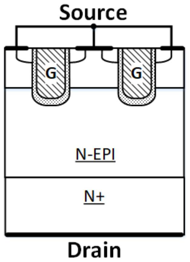
[0056] (4) if Figure 6 As shown, two N-grooves are formed from the top of the device to the N-buried layer, and the N-buried layer is drawn out as a drain, and...


PUM


Abstract

The invention relates to a trench gate field effect transistor with a charge balance structure and a manufacturing method thereof, belonging to the technical field of semiconductors. Using the manufacturing method of the present invention, a layer of N-buried region and P-buried region are buried in N-EPI, N-buried region is mainly used to reduce via resistance, and P-buried region is used to assist N-buried region in The depletion in the off state forms a charge balance structure, and then leads the drain of the vertical device to the upper surface of the device through the N-buried layer and the N-trench to form a planar device, which can be better integrated in the circuit. Moreover, the trench gate field effect transistor with charge balance structure of the present invention has simple production process, relatively low cost and wide application range.

Description

technical field [0001] The invention relates to the technical field of semiconductors, in particular to the technical field of field effect transistors, and specifically refers to a trench gate field effect transistor with a charge balance structure and a manufacturing method thereof. Background technique [0002] With the rapid development of electronic information technology, especially the rapid development of fashion consumer electronics and portable products, the demand for power devices such as metal oxide semiconductor field effect transistors (MOSFETs) is increasing. MOSFETs are mainly divided into horizontal and vertical Two, the obvious advantage of the lateral MOSFET is its better integration, which can be more easily integrated into the process platform of the existing technology, but because its withstand voltage drift region is spread out on the surface, it shows its biggest shortcoming, occupying The larger the area, the area represents the cost, and the highe...

Claims


Application Information

Patent Timeline
Patent Type & Authority Patents(China)
IPC IPC(8): H01L21/336H01L29/06H01L29/78
CPCH01L29/0634H01L29/66484H01L29/66734H01L29/7813H01L29/7831
Inventor 张帅黄昕
Owner 济南安海半导体有限公司
Why Eureka
Try Eureka