Copper interconnection layer and Damascus process method of copper interconnection layer

A process method, copper interconnection technology, applied in the direction of semiconductor/solid-state device components, semiconductor devices, electrical components, etc., can solve problems such as poor results

Pending Publication Date: 2022-07-08
SIEN QINGDAO INTEGRATED CIRCUITS CO LTD
View PDF0 Cites 0 Cited by
  • Summary
  • Abstract
  • Description
  • Claims
  • Application Information

AI Technical Summary

Problems solved by technology

However, with the continuous reduction of CMOS in BEOL, the traditional Ta / TaN liner and barrier layers for copper interconnection in dual damascene (DD) structure are effective in preventing Cu diffusion, reducing via resistance, and the interaction with Cu. Adhesion to achieve Electron Migration (EM) properties of Cu is poor

Method used


Image

  • Copper interconnection layer and Damascus process method of copper interconnection layer
  • Copper interconnection layer and Damascus process method of copper interconnection layer
  • Copper interconnection layer and Damascus process method of copper interconnection layer

Examples


Embodiment 1

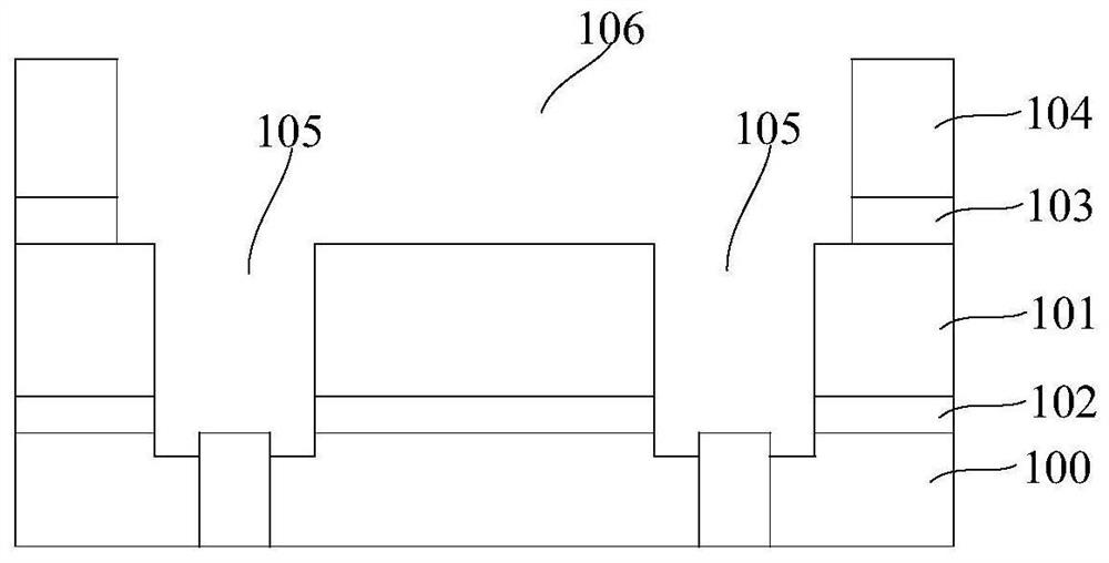
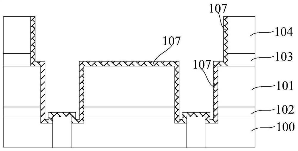
[0075] In the process of forming the copper interconnect layer by the Damascus process, such as Figure 14 As shown, the copper interconnect layer is formed in the dielectric layer 02 above the substrate 01, the dielectric layer is usually a low-k dielectric layer, and the copper 04 in the copper interconnect layer is easily migrated to the surrounding low-k dielectric layer or Diffusion, which in turn reduces the electron transport properties of copper. In order to prevent the migration or diffusion of copper to the dielectric layer, the barrier layer 03 is usually formed on the sidewall of the through hole or the trench where the interconnect layer is formed in the prior art. like Figure 14 As shown, taking a through hole as an example, a metal barrier layer 03 is formed on the sidewall and bottom of the through hole, and the barrier layer is usually Ta, TaN or Ta and TaN stack. In the conventional through interconnect layer, the above-mentioned metal barrier layer can ef...

Embodiment 2

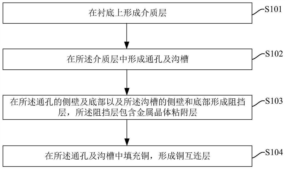
[0093] The present embodiment also provides a damascene process method for a copper interconnection layer, forming a barrier layer including a metal crystal adhesion layer on the sidewalls and bottoms of the through holes and trenches where the copper interconnection layer is formed, so as to effectively prevent copper from entering the surrounding dielectric. Layer migration and diffusion. like Figure 9 As shown, the method includes the following steps:

[0094] Step S201: forming a dielectric layer on the substrate;

[0095] Step S202: forming through holes and trenches in the dielectric layer;

[0096] Step S203: forming a barrier layer on the sidewall and bottom of the through hole and the sidewall and bottom of the trench, the barrier layer comprising a graphene layer; and

[0097] Step S204 : filling the through holes and trenches with copper to form a copper interconnection layer.

[0098] The above steps S201 , S202 and S204 are the same as the steps S101 , S102 a...


PUM

PropertyMeasurementUnit
thicknessaaaaaaaaaa
thicknessaaaaaaaaaa
thicknessaaaaaaaaaa

Abstract

The invention provides a copper interconnection layer and a Damascus process method of the copper interconnection layer. And barrier layers are formed on the side walls and the bottoms of the through holes and the grooves for forming the copper interconnection lines, and each barrier layer comprises a metal crystal adhesion layer or a graphene layer. The metal crystal adhesion layer can be a crystal Co layer or a crystal Ru layer or a crystal Os layer. The metal crystal adhesion layer can enhance the adhesion with Cu, effectively inhibits diffusion of Cu into the dielectric layer, and is beneficial to improving the electron migration performance of Cu. The formation of the metal crystal adhesion layer can effectively reduce the total thickness of the barrier layer and the first barrier layer, and effectively reduce the resistance of the through hole. The graphene layer is an amorphous carbon / graphene composite layer. Due to the formation of the graphene layer, the Cu interconnection layer has lower resistivity, and the formation of the graphene layer can also effectively reduce the total thickness of the barrier layer or the barrier layer and the first barrier layer, so that the resistance of the through hole is effectively reduced.

Description

technical field [0001] The invention relates to the field of semiconductor devices, in particular to a copper interconnection layer and a Damascus process method for the copper interconnection layer. Background technique [0002] The resistance–capacitance (RC) delay of interconnect circuits is a major factor affecting the speed performance of logic circuits. Since the 0.13μm CMOS technology node, copper (Cu) has been used as an interconnect material due to its lower resistivity. However, Cu easily diffuses into low-k dielectrics and also reduces the Electro-migration (EM) performance of Cu. [0003] In the traditional process, Ta / TaN is usually used as the barrier layer of the Cu interconnect layer in the double damascene process to prevent the diffusion of Cu. However, as CMOS in BEOL continues to decrease, the traditional Ta / TaN liner and barrier layers used for copper interconnects in dual damascene (DD) structures are preventing Cu diffusion, reducing through-hole res...

Claims


Application Information

Patent Timeline
Patent Type & Authority Applications(China)
IPC IPC(8): H01L21/768H01L23/538
CPCH01L21/76807H01L21/76843H01L23/5386H01L23/53238H01L21/76844H01L21/76846H01L23/5226H01L21/76877H01L21/76802
Inventor 孟昭生吴荘荘季明华
Owner SIEN QINGDAO INTEGRATED CIRCUITS CO LTD
Why Eureka
Try Eureka