Method for precision cleaning and drying flat objects

Active Publication Date: 2009-02-05
PLANAR SEMICON CORP PTE LTD
View PDF14 Cites 33 Cited by
  • Summary
  • Abstract
  • Description
  • Claims
  • Application Information

AI Technical Summary

Benefits of technology

[0023]It is an object of the present invention to provide a method for cleaning and sequentially drying a vertically oriented semiconductor wafer substrate to high precision in a single working chamber without changing the position of the substrate in transfer from cleaning to drying. It is another object to perform cleaning in a jet-pulse mode of emission of the cleaning liquid with rotation of the wafer substrate and to continue dryi

Problems solved by technology

It is well known that presence of chemical contaminants and particles of impurities may significantly reduce the yield of the products and noticeably affect the performance and reliability of the produced semiconductor devices.
Hydrophobic substrate is more difficult to clean than hydrophilic substrate because of its poor wettability with aqueous cleaning solutions.
Normally, after various processes of chemical treatment, wafer substrates are cleaned with de-ionized water, the efficiency of which is very low.
Drying of hydrophobic wafers is even more challenging than cleaning because of the high affinity of particle contaminants to hydrophobic surfaces.
These waterma

Method used


Image

  • Method for precision cleaning and drying flat objects
  • Method for precision cleaning and drying flat objects
  • Method for precision cleaning and drying flat objects

Examples


Embodiment Construction

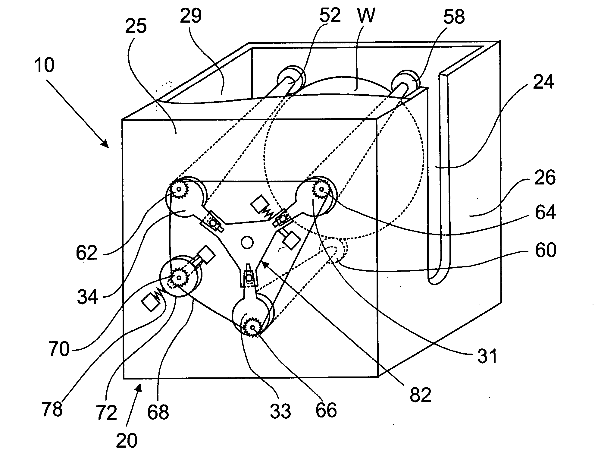
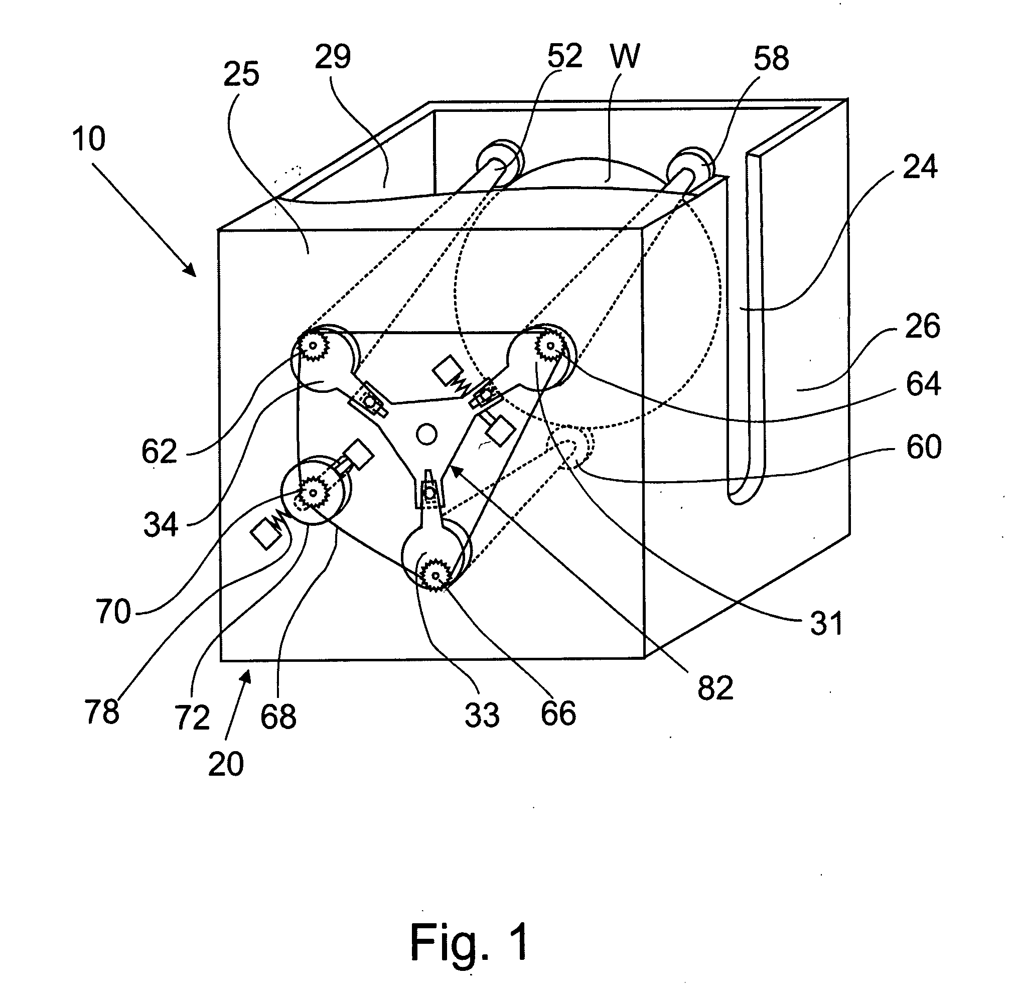
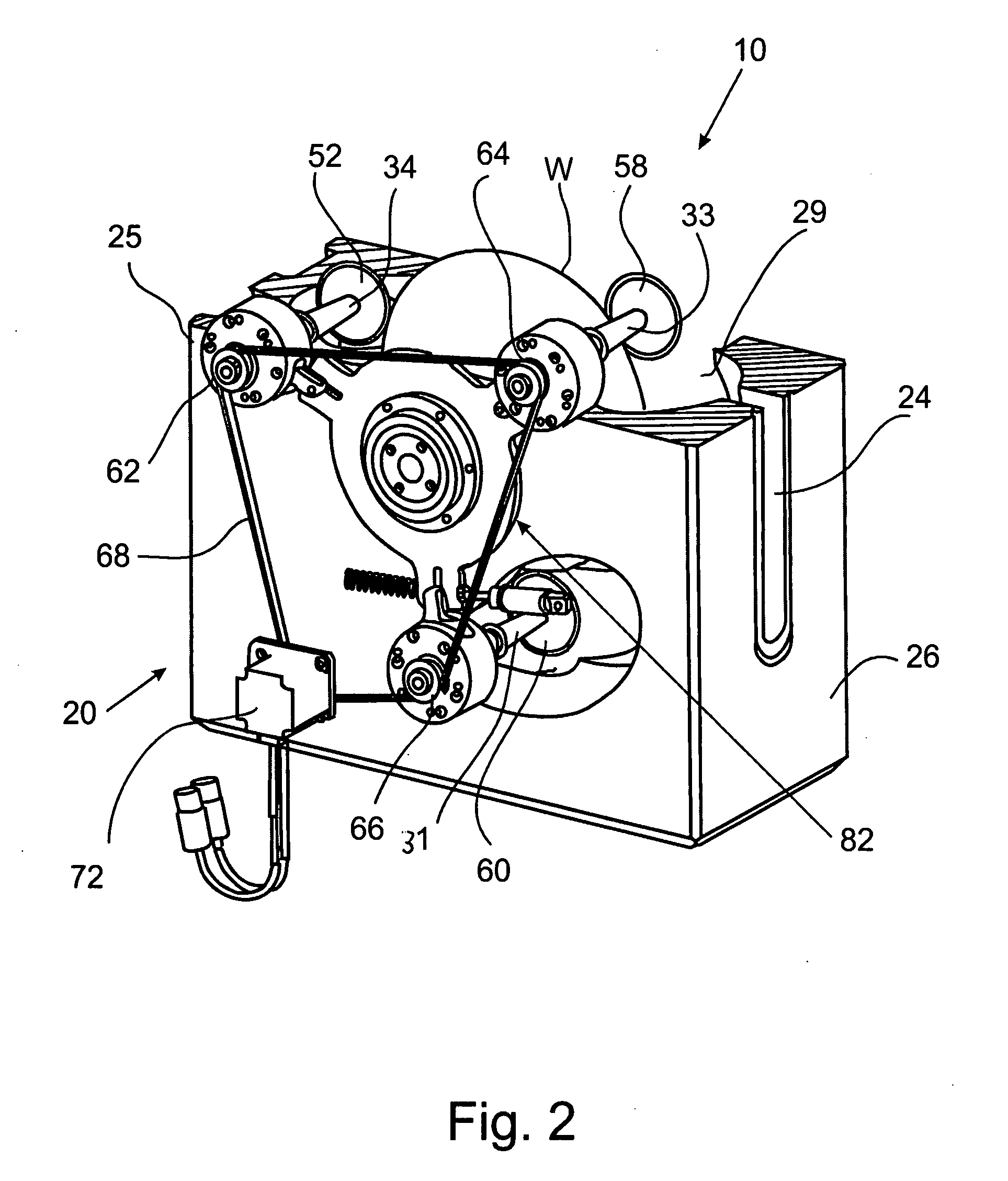
[0047]A simplified three-dimensional sectional view of a single-chamber apparatus of the present invention for precision cleaning and drying of flat objects, such as semiconductor substrates, is shown in FIG. 1. FIG. 2 is a three-dimensional view of the rear side of the apparatus with the showerhead removed, illustrating external and internal parts of the mechanism for rotating the wafer-driving rollers.

[0048]Although the invention relates more specifically to a mechanism for precision drying, it would be useful first to describe the single-chamber cleaning and drying apparatus of the invention as a whole with all the driving, loading, and unloading mechanisms, as well as other mechanisms and devices, which, in general, have been described in earlier pending U.S. patent application Ser. No. ______ and which are almost entirely incorporated into the apparatus of the present invention.

[0049]The apparatus, which as a whole is designated by reference numeral 10, is shown in FIG. 1 with ...


PUM


Abstract

Cleaning and drying of semiconductor wafers is carried out in a single-chamber type cleaning/drying apparatus for flat objects such as semiconductor wafer, where cleaning is carried out by impinging both sides of the wafer which rotates at a relatively low speed with jets of a washing liquid and where subsequent drying is carried out in the same chamber by increasing the rotation speed of the wafer and supplying an isopropyl-alcohol (IPA) mist onto the wafer from the top of the chamber. After the IPA forms a solution with the residue of water on the wafer, the drying process is accelerated by supplying gaseous nitrogen through nozzles arranged on both side of the coaxial with the wafer center. As a result, the IPA-water solution quickly evaporates without leaving traces of water drops on the dried surface.

Description

CROSS-REFERENCE TO RELATED APPLICATIONS[0001]The present patent application is related to a co-pending patent application Ser. No. ______ filed by the same applicants and entitled: “A SINGLE-CHAMBER APPARATUS FOR PRECISION CLEANING AND DRYING FLAT OBJECTS”.FIELD OF THE INVENTION[0002]The present invention relates to semiconductor manufacture, in particular to a method for precision cleaning and drying flat objects, such as semiconductor-wafer substrates. More specifically, the invention relates to a method of cleaning and drying semiconductor-wafer substrates in a single-chamber apparatus equipped with pulsed-jet cleaning nozzles for liquid cleaning and with means for formation and supply of a mist of isopropyl alcohol and a flow of gaseous nitrogen to an object for drying the latter.DESCRIPTION OF THE PRIOR ART[0003]Cleaning and drying of surfaces of wafer substrates is one of the most important steps in the fabrication of semiconductor microelectronic devices. It is well known tha...

Claims


Application Information

Patent Timeline
IPC IPC(8): B08B7/04
CPCB08B3/02H01L21/67028B08B11/02H01L21/02052
Inventor RANDHAWA, RUBINDERSAJJAD, BASHAEREZ, SHMUELCHRISTOV, HARRY
Owner PLANAR SEMICON CORP PTE LTD
Why Eureka
Try Eureka