SiGe DIAC ESD protection structure

Active Publication Date: 2009-02-05
NAT SEMICON CORP
View PDF7 Cites 28 Cited by
  • Summary
  • Abstract
  • Description
  • Claims
  • Application Information

AI Technical Summary

Problems solved by technology

However, when the voltage across the DIAC exceeds the breakdown voltage, the DIAC becomes conductive, providing a low-resistance current path between the two nodes.

Method used


Image

  • SiGe DIAC ESD protection structure
  • SiGe DIAC ESD protection structure
  • SiGe DIAC ESD protection structure

Examples


Embodiment Construction

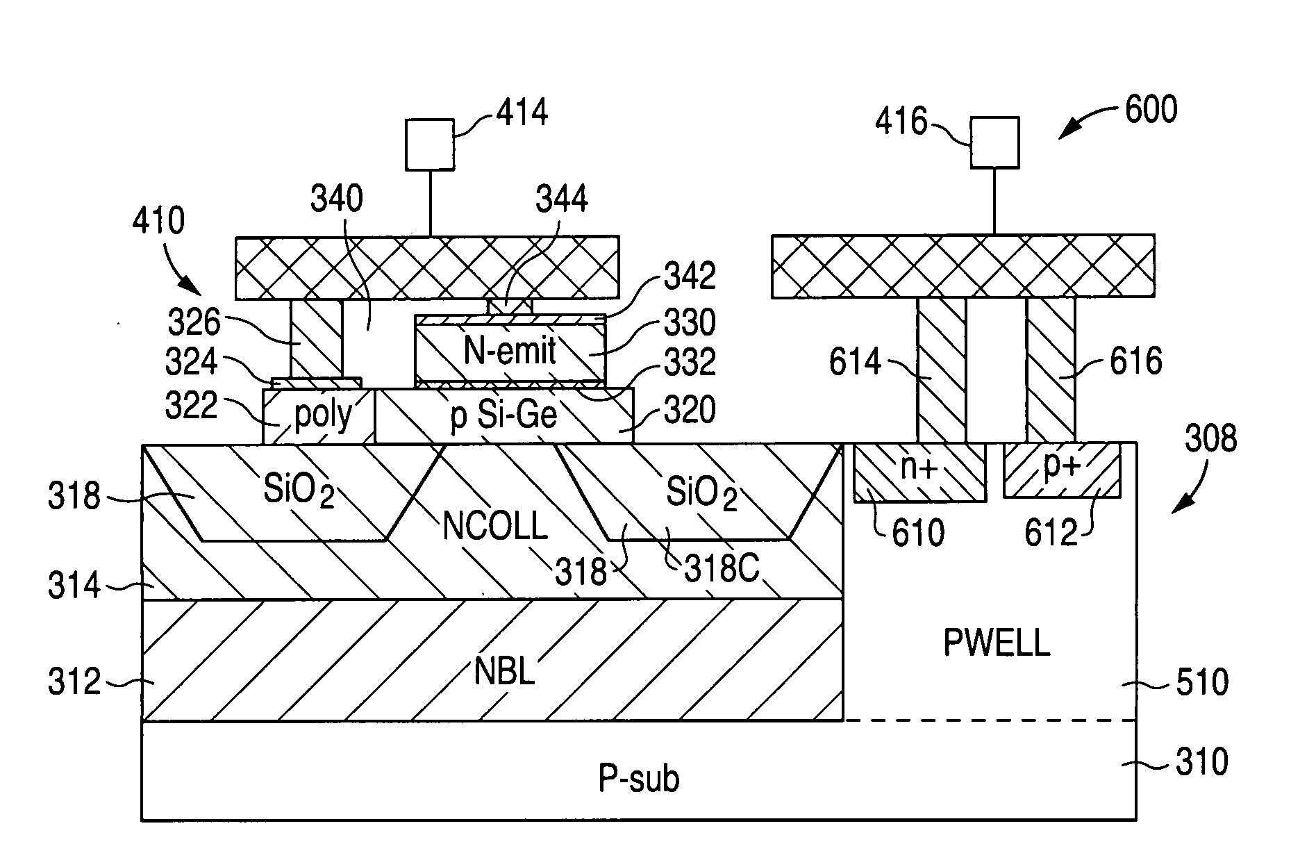
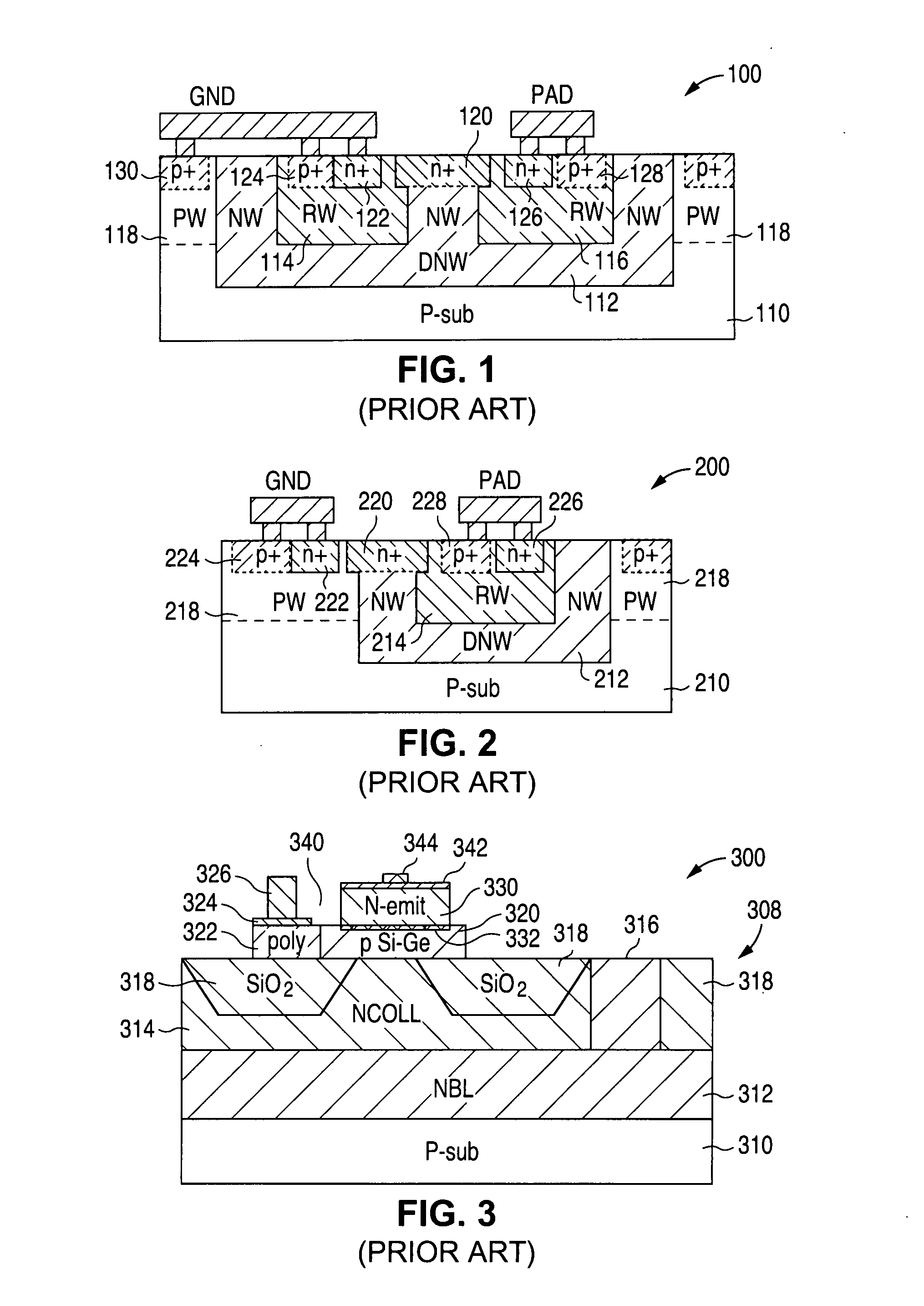
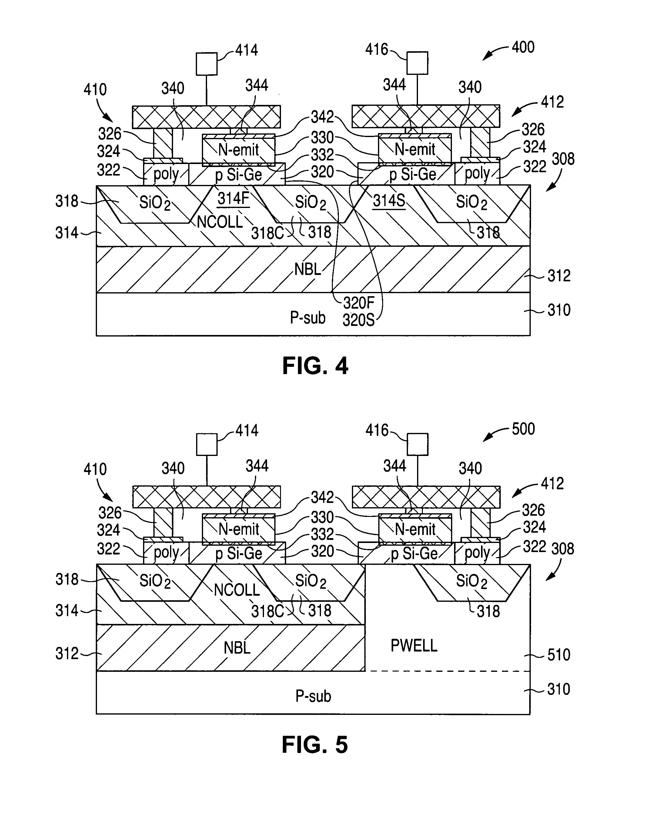
[0027]FIG. 4 shows a cross-sectional view that illustrates an example of a SiGe DIAC ESD protection structure 400 in accordance with the present invention. Structure 400 is similar to transistor 300 and, as a result, utilizes the same reference numerals to designate the elements which are common to structure 400 and transistor 300.

[0028]As shown in FIG. 4, SiGe DIAC ESD protection structure 400 includes semiconductor structure 308 which has a p− substrate 310, and an n+ buried layer 312 that touches and lies over p− substrate 310. In addition, semiconductor structure 308 includes an n-type collector region 314 that touches the top surface of n+ buried layer 312, and a number of shallow trench isolation regions 318 that extend down from the top surface of semiconductor structure 308.

[0029]As further shown in FIG. 4, structure 400 also includes a pair of spaced-apart base / emitter structures 410 and 412 that are formed on the top surface of semiconductor structure 308 to touch n-type c...


PUM


Abstract

A diode for alternating current (DIAC) electrostatic discharge (ESD) protection circuit is formed in a silicon germanium (SiGe) hetrojunction bipolar transistor (HBT) process that utilizes a very thin collector region. ESD protection for a pair of to-be-protected pads is provided by utilizing the base structures and the emitter structures of the SiGe transistors.

Description

BACKGROUND OF THE INVENTION[0001]1. Field of the Invention[0002]The present invention relates to a DIAC ESD protection structure and, more particularly, to a SiGe DIAC ESD protection structure.[0003]2. Description of the Related Art[0004]A diode for alternating current (DIAC) is a bidirectional diode that is commonly used in alternating current (AC) applications. In operation, when the voltage across a DIAC is less than a breakdown voltage, the DIAC is substantially non-conductive, providing a high-resistance current path between two nodes.[0005]However, when the voltage across the DIAC exceeds the breakdown voltage, the DIAC becomes conductive, providing a low-resistance current path between the two nodes. The DIAC continues to provide a low-resistance current path until the current flowing through the DIAC falls below a holding current, at which time the DIAC switches back and again provides a high-resistance current path. Because of these operational characteristics, DIAC structu...

Claims


Application Information

Patent Timeline
Patent Type & Authority Applications(United States)
IPC IPC(8): H01L29/74H01L21/332
CPCH01L27/0259
Inventor VASHCHENKO, VLADISLAVHOPPER, PETER J.
Owner NAT SEMICON CORP
Why Eureka
Try Eureka