Programmable via devices in back end of line level

a technology of programmable via and back end, applied in the field of reconfigurable circuits, can solve the problems and achieve the effect of solving the problem of integrating programmable via technology with existing semiconductor architectur

Active Publication Date: 2009-02-05
GLOBALFOUNDRIES US INC
View PDF12 Cites 26 Cited by
  • Summary
  • Abstract
  • Description
  • Claims
  • Application Information

AI Technical Summary

Benefits of technology

[0011]In still another aspect of the invention, an integrated logic circuit is provided. The integrated logic circuit comprises a plurality of logic blocks; and at least one programmable via device interconnecting two or more of the logic blocks. The programmable via device comprises a first dielectric layer; at least one isolation layer over the first dielectric layer; a heater within the isolation layer; a capping layer over a side of the isolation layer opposite the first dielectric layer; at least one programmable via extending through the capping layer and at least a portion of the isolation layer and in contact with the heater, the programmable via comprising at least one phase change material; a conductive cap over the programmable via; a second dielectric layer over a side of the capping layer opposite the isolation layer; a first conductive via and a second conductive via, each extending through the second dielectric layer, the capping layer and at least a portion of the isolation layer and in contact with the heater; and a third conductive via extending through the second dielectric layer and in contact with the conductive cap.

Problems solved by technology

Integrating programmable via technology with existing semiconductor architecture still presents a challenge, however, especially in the context of scaled process technology.
For example, undesirable interactions of programmable via components with commonly employed semiconductor device materials can affect device performance, and thus present a problem.

Method used


Image

  • Programmable via devices in back end of line level
  • Programmable via devices in back end of line level
  • Programmable via devices in back end of line level

Examples


Embodiment Construction

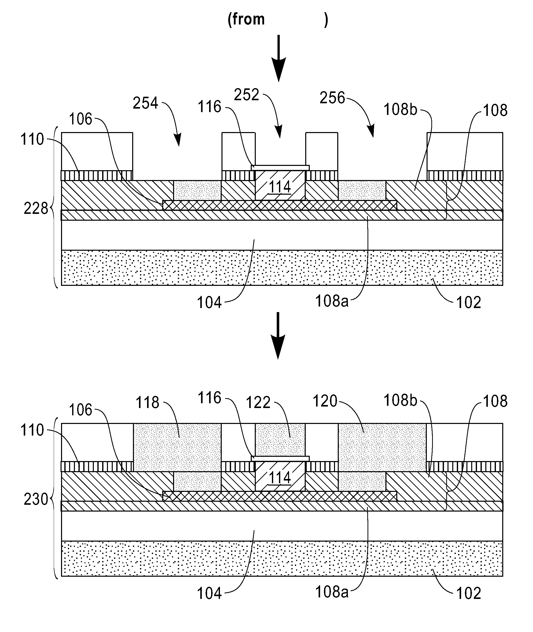
[0022]FIG. 1 is a diagram illustrating exemplary semiconductor chip 100. Semiconductor chip 100 comprises programmable via device 101 placed in a back end of line (BEOL) level thereof, i.e., over device layer 102. As will be described in detail below, the configuration of programmable via device 101 makes programmable via device 101 integratable with BEOL levels of a semiconductor chip.

[0023]The term “BEOL,” as used herein, generally refers to a stage(s) of production of a semiconductor chip after first metallization. As such, the term “BEOL levels,” as used herein, generally refers to portions, i.e., levels and / or layers, associated with a semiconductor chip after first metallization. Further, any portions, i.e., levels and / or layers, of the semiconductor chip fabricated up to, and including, first metallization (also known as front end of line “FEOL” levels) are collectively referred to herein as a “device layer(s).” Placing the programmable via device in BEOL levels of a chip is ...


PUM


Abstract

Programmable via devices and methods for the fabrication thereof are provided. In one aspect, a programmable via device is provided. The programmable via device comprises a first dielectric layer; at least one isolation layer over the first dielectric layer; a heater within the isolation layer; a capping layer over a side of the isolation layer opposite the first dielectric layer; at least one programmable via extending through the capping layer and at least a portion of the isolation layer and in contact with the heater, the programmable via comprising at least one phase change material; a conductive cap over the programmable via; a second dielectric layer over a side of the capping layer opposite the isolation layer; a first conductive via and a second conductive via, each extending through the second dielectric layer, the capping layer and at least a portion of the isolation layer and in contact with the heater; and a third conductive via extending through the second dielectric layer and in contact with the conductive cap.

Description

CROSS-REFERENCE TO RELATED APPLICATIONS[0001]This application is related to the commonly owned U.S. application Ser. No. 11 / 770,455, entitled “CMOS-Process-Compatible Programmable Via Device,” designated as Attorney Reference Number YOR920070282US1, filed on Jun. 28, 2007, the commonly owned U.S. application Ser. No. 11 / 776,295, entitled “Four-Terminal Reconfigurable Devices,” designated as Attorney Reference Number YOR920070283US1, filed on Jul. 11, 2007, and the commonly owned U.S. application Ser. No. ______, entitled “Programmable Via Devices With Air Gap Isolation,” designated as Attorney Reference Number YOR920070287US1, filed herewith on the same day of ______. The contents of the preceding applications are incorporated herein by reference as fully set forth herein.FIELD OF THE INVENTION[0002]The present invention relates to reconfigurable circuits, and more particularly, to programmable via devices and methods for fabrication thereof. Background of the Invention[0003]Reconfi...

Claims


Application Information

Patent Timeline
Patent Type & Authority Applications(United States)
IPC IPC(8): H01L45/00H03K19/177
CPCH01L28/20H01L45/06H01L45/1206H01L45/122Y10S977/754H01L45/144H01L45/148H01L45/1683H01L28/65H01L45/1286H10N70/253H10N70/821H10N70/8613H10N70/231H10N70/884H10N70/066H10N70/8828
Inventor CHEN, KUAN-NENGKRUSIN-ELBAUM, LIANEWNS, DENNIS M.PURUSHOTHAMAN, SAMPATH
Owner GLOBALFOUNDRIES US INC
Why Eureka
Try Eureka