Device for thorough testing of secure electronic components

a technology for electronic components and devices, applied in the direction of testing circuits, resistance/reactance/impedence, instruments, etc., can solve the problems of inadvertent disclosure of the contents of the secure logic, unauthorized users could circumvent the rules, and use the devices without authorization,

Inactive Publication Date: 2009-02-05
AVAGO TECH WIRELESS IP SINGAPORE PTE
View PDF3 Cites 0 Cited by
  • Summary
  • Abstract
  • Description
  • Claims
  • Application Information

AI Technical Summary

Benefits of technology

[0010]The present invention concerns an apparatus including a test circuit, an output circuit and a control circuit. The test circuit may be configured to generate test data in response to one or more test vectors. The output circuit may be configured to present data in a first mode and prevent presentation of data in a second mode. The output circuit may be configured to switch between the first mode and the second mode in response to a control signal. The control circuit may be configured to generate the control signal according to predetermined criteria for protecting secure data within the apparatus while allowing the test data to be presented.
[0011]The objects, features and advantages of the present invention include providing a method and / or apparatus for thorough testing of secure electronic components that may (i) clear out contents of all secure logic before testing begins, (ii) prevent a device from entering a test mode until all of the secure data is removed, (iii) allow only the contents of the device that result from testing to be visible to a user, (iv) work with scan chains and / or (v) disable outputs of a device until secure data is destroyed.

Problems solved by technology

However, if the unauthorized users could review the rules that disallow the unauthorized users from using the secure electronic device, the unauthorized users could circumvent the rules and use the device without authorization.
In particular, during thorough testing of the secure electronic devices, it is possible to inadvertently divulge the contents of the secure logic.

Method used


Image

  • Device for thorough testing of secure electronic components
  • Device for thorough testing of secure electronic components
  • Device for thorough testing of secure electronic components

Examples


Embodiment Construction

[0018]The present invention generally provides a method and / or an apparatus for clearing out the contents of all secure logic before testing of a device (or chip) begins. In one example, the device being tested may be prevented from entering into a test mode until all of the secure data has been removed from the device. Once testing begins, only the contents of the device that result from the tests applied may be visible to any user. The present invention may prevent users from determining any secret (or secure) information contained within a device.

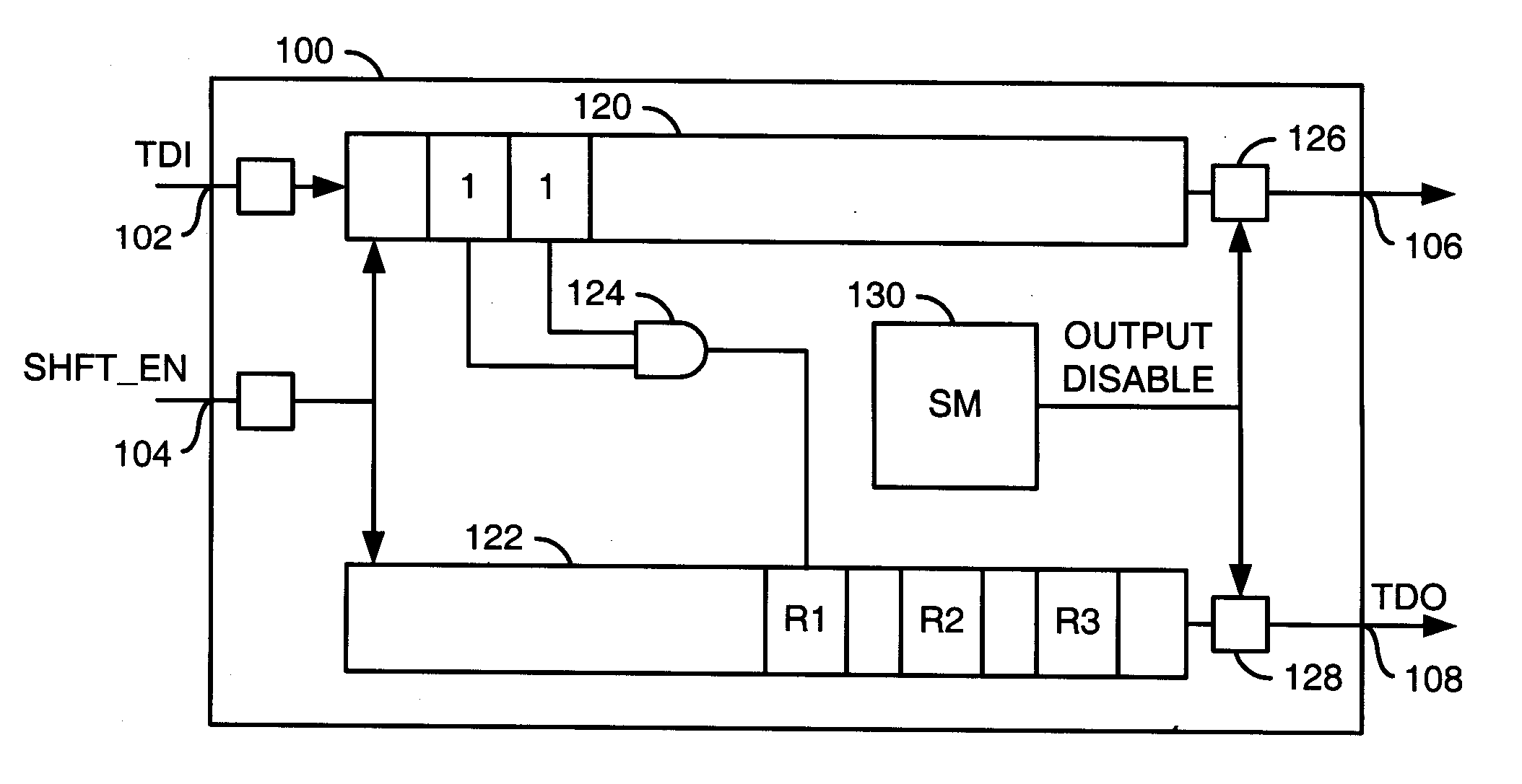
[0019]Referring to FIG. 2, a diagram is shown illustrating a secure electronic device 100 implemented in accordance with a preferred embodiment of the present invention. In one example, the device 100 may have an input 102, an input 104, an output 106 and an output 108. The input 102 may be configured to receive test vector data (e.g., TDI). The input 104 may be configured to receive a test shift enable signal (e.g., SHFT_EN). The output...


PUM


Abstract

An apparatus including a test circuit, an output circuit and a control circuit. The test circuit may be configured to generate test data in response to one or more test vectors. The output circuit may be configured to present data in a first mode and prevent presentation of data in a second mode. The output circuit may be configured to switch between the first mode and the second mode in response to a control signal. The control circuit may be configured to generate the control signal according to predetermined criteria for protecting secure data within the apparatus while allowing the test data to be presented.

Description

[0001]This application claims the benefit of U.S. Provisional Application No. 60 / 963,287, filed Aug. 17, 2007 and is hereby incorporated by reference in its entirety.FIELD OF THE INVENTION[0002]The present invention relates to electronic device testing generally and, more particularly, to a method and / or apparatus for thorough testing of secure electronic components.BACKGROUND OF THE INVENTION[0003]Secure electronic devices can be designed for use by select users. Unauthorized users who are not permitted to use the secure electronic device are prevented from using the device by logic within the device. However, if the unauthorized users could review the rules that disallow the unauthorized users from using the secure electronic device, the unauthorized users could circumvent the rules and use the device without authorization.[0004]In particular, during thorough testing of the secure electronic devices, it is possible to inadvertently divulge the contents of the secure logic. Despite...

Claims


Application Information

Patent Timeline
Patent Type & Authority Applications(United States)
IPC IPC(8): G01R31/3177
CPCG01R31/318544G01R31/318536
Inventor PEARSON, ERIC C.HOWARD, MICHAEL A.
Owner AVAGO TECH WIRELESS IP SINGAPORE PTE
Why Eureka
Try Eureka