Handling defective memory blocks of NAND memory devices

a technology of nand memory devices and defective blocks, applied in static storage, digital storage, instruments, etc., can solve problems such as shortening between word lines and bit lines, and defective blocks can occur

Active Publication Date: 2005-12-29
MICRON TECH INC
View PDF9 Cites 12 Cited by
  • Summary
  • Abstract
  • Description
  • Claims
  • Application Information

AI Technical Summary

Benefits of technology

[0013] For another embodiment, the invention provides a NAND memory device having a memory array with a plurality of memory blocks, a block select circuit coupled to each of the memory blocks, a decoder coupled to each of the block select circuits, and a volatile latch coupled to each of the decoders and each of the block select circuits and thereby coupled to each of the memory blocks. Each volatile latch is adapted to selectively prevent activation of the respective block select circuit coupled thereto so as to prevent testing of the memory block coupled to that block select circuit when that memory block is a known defective block.
[0014] For another embodiment, the invention provides a NAND memory device having a memory array with a plurality of memory blocks, a block select circuit coupled to each of the

Problems solved by technology

However, each memory cell is not directly connected to a column bit line by its drain region.
Defective blocks can occur during the manufacture of a flash memory array having rows and columns of memory cells.
Typical defects can include bad memory cells, open circuits, shorts between a pair of rows, and shorts between a word line and bit line.
For NOR memory devices, defective blocks are usually unacceptable, and redundant elements are often us

Method used


Image

  • Handling defective memory blocks of NAND memory devices
  • Handling defective memory blocks of NAND memory devices
  • Handling defective memory blocks of NAND memory devices

Examples


Embodiment Construction

[0021] In the following detailed description of the invention, reference is made to the accompanying drawings that form a part hereof, and in which is shown, by way of illustration, specific embodiments in which the invention may be practiced. In the drawings, like numerals describe substantially similar components throughout the several views. These embodiments are described in sufficient detail to enable those skilled in the art to practice the invention. Other embodiments may be utilized and structural, logical, and electrical changes may be made without departing from the scope of the present invention. The following detailed description is, therefore, not to be taken in a limiting sense, and the scope of the present invention is defined only by the appended claims and equivalents thereof.

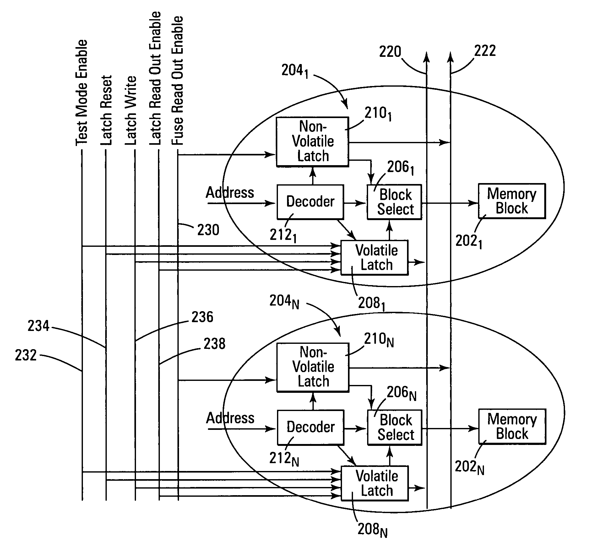
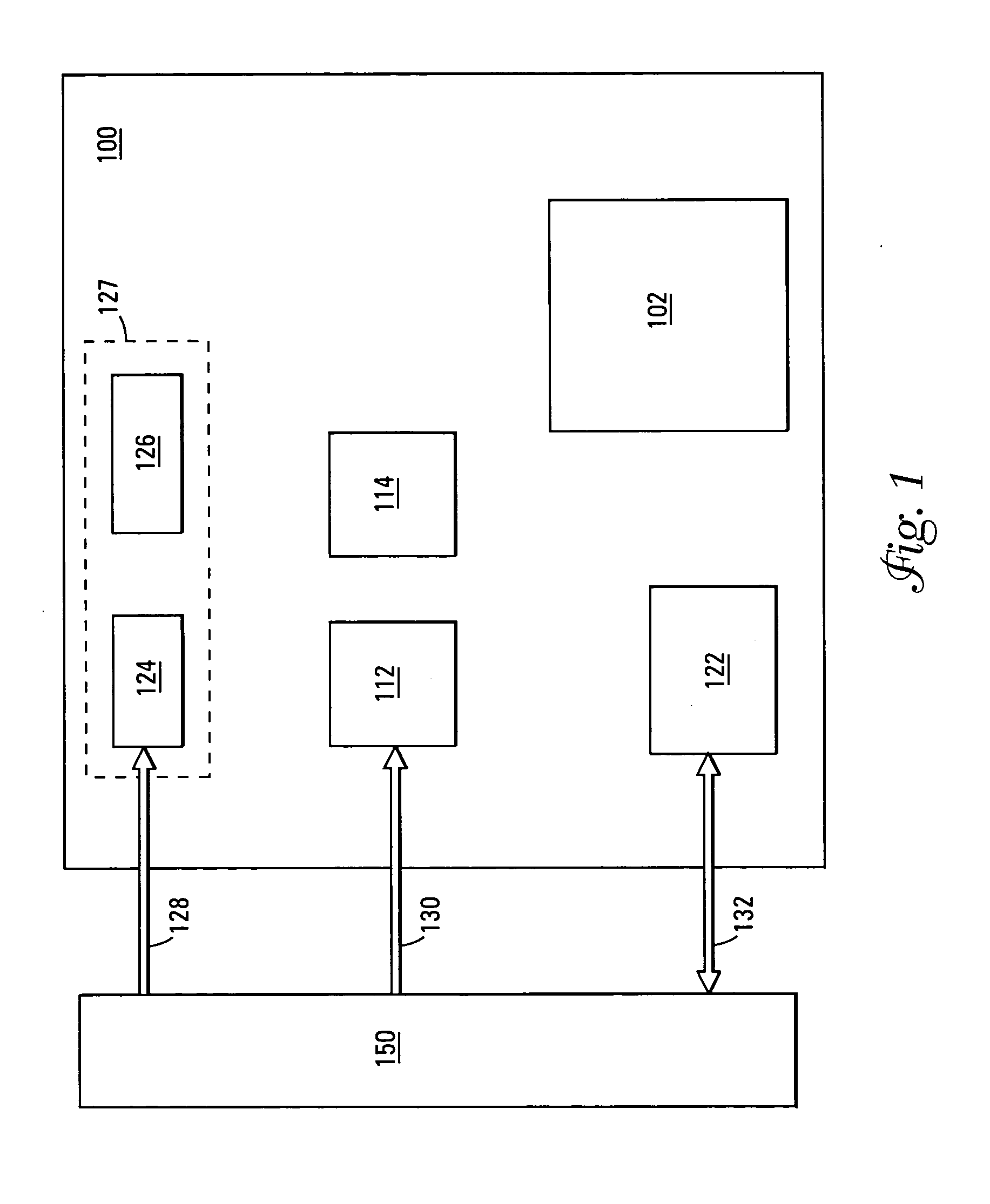
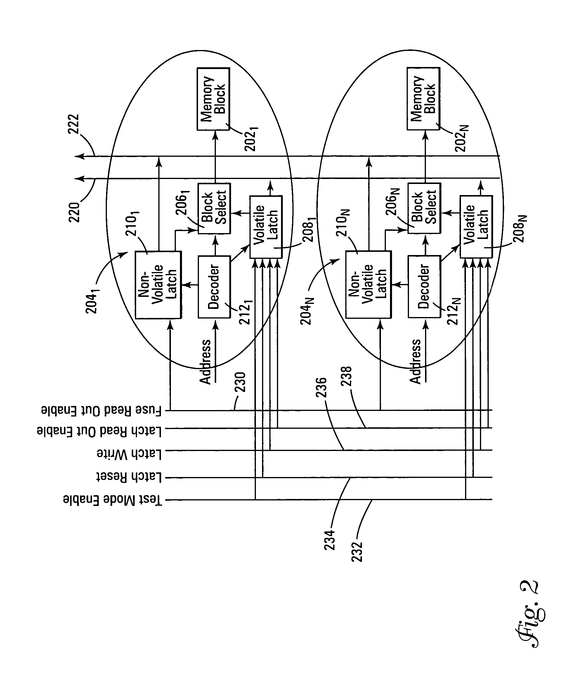
[0022]FIG. 1 is a block diagram illustration of a portion of a NAND flash memory device 100 according to an embodiment of the present invention. Memory device 100 includes a memory array 102 h...


PUM


Abstract

Apparatus and methods are provided. A NAND memory device has a memory array comprising a plurality of memory blocks and a volatile latch coupled to each of the memory blocks for selectively preventing testing of the respective memory block coupled thereto when that memory block is a known defective block. A non-volatile latch may also be coupled to each of the memory blocks for permanently preventing access, during normal operation of the memory device, to the respective memory block coupled thereto when that memory block is a known defective block.

Description

TECHNICAL FIELD OF THE INVENTION [0001] The present invention relates generally to NAND memory devices and in particular the present invention relates to handling defective memory blocks of NAND memory devices. BACKGROUND OF THE INVENTION [0002] Memory devices are typically provided as internal storage areas in computers. The term memory identifies data storage that comes in the form of integrated circuit chips. In general, memory devices contain an array of memory cells for storing data, and row and column decoder circuits coupled to the array of memory cells for accessing the array of memory cells in response to an external address. [0003] One type of memory is a non-volatile memory known as flash memory. A flash memory is a type of EEPROM (electrically-erasable programmable read-only memory) that can be erased and reprogrammed in blocks. Many modern personal computers (PCs) have their BIOS stored on a flash memory chip so that it can easily be updated if necessary. Such a BIOS is...

Claims


Application Information

Patent Timeline
IPC IPC(8): G11C8/02G11C16/04G11C29/00G11C29/26
CPCG11C29/832G11C2029/4402G11C16/04G11C29/82G11C29/26G11C29/789G11C16/0483
Inventor LOUIE, BENJAMINYIP, AARON
Owner MICRON TECH INC
Why Eureka
Try Eureka