Semiconductor integrated circuit and bist circuit design method

a semiconductor integrated circuit and design method technology, applied in error detection/correction, instruments, measurement devices, etc., can solve the problems of difficult to conduct a sufficient test for the semiconductor integrated circuit from outside, large overhead area of the circuit, and small number of external input/output terminals, etc., to achieve the effect of improving the test speed of the bis

Inactive Publication Date: 2008-02-14
PANASONIC CORP
View PDF8 Cites 10 Cited by
  • Summary
  • Abstract
  • Description
  • Claims
  • Application Information

AI Technical Summary

Benefits of technology

[0025]The method for designing a BIST circuit according to the present invention with the stated structure is capable of inserting the register circuit if the interconnect delay time between the macro cells on the signal line connecting the testing circuit and the memory circuits is longer than the testing time of the memory circuits. Accordingly, it is possible to design a circuit that is capable of improving the test speed of the BIST by providing the test vectors in accordance with the interconnect delay time that occurs between the testing circuit and the register circuit or the register circuit and the memory circuit.

Problems solved by technology

Due to such high integration, the number of external input / output terminals is comparatively small for its circuit size, and it is difficult to conduct a sufficient test for the semiconductor integrated circuit from outside.
However, it is necessary for the BIST to provide a circuit block only for the test, and this causes an area overhead on the circuit.
However, with the structure disclosed by the Document 1, since the BIST circuit provides a plurality of SRAMs with a test vector, the length of a wire led to an SRAM placed away from the BIST circuit is long, and an interconnect delay becomes large.
Therefore, the test speed is limited to the interconnect delay speed, and it is impossible to conduct a test at an original speed of the memory circuit, that is, so called an at-speed test.

Method used


Image

  • Semiconductor integrated circuit and bist circuit design method
  • Semiconductor integrated circuit and bist circuit design method
  • Semiconductor integrated circuit and bist circuit design method

Examples


first embodiment

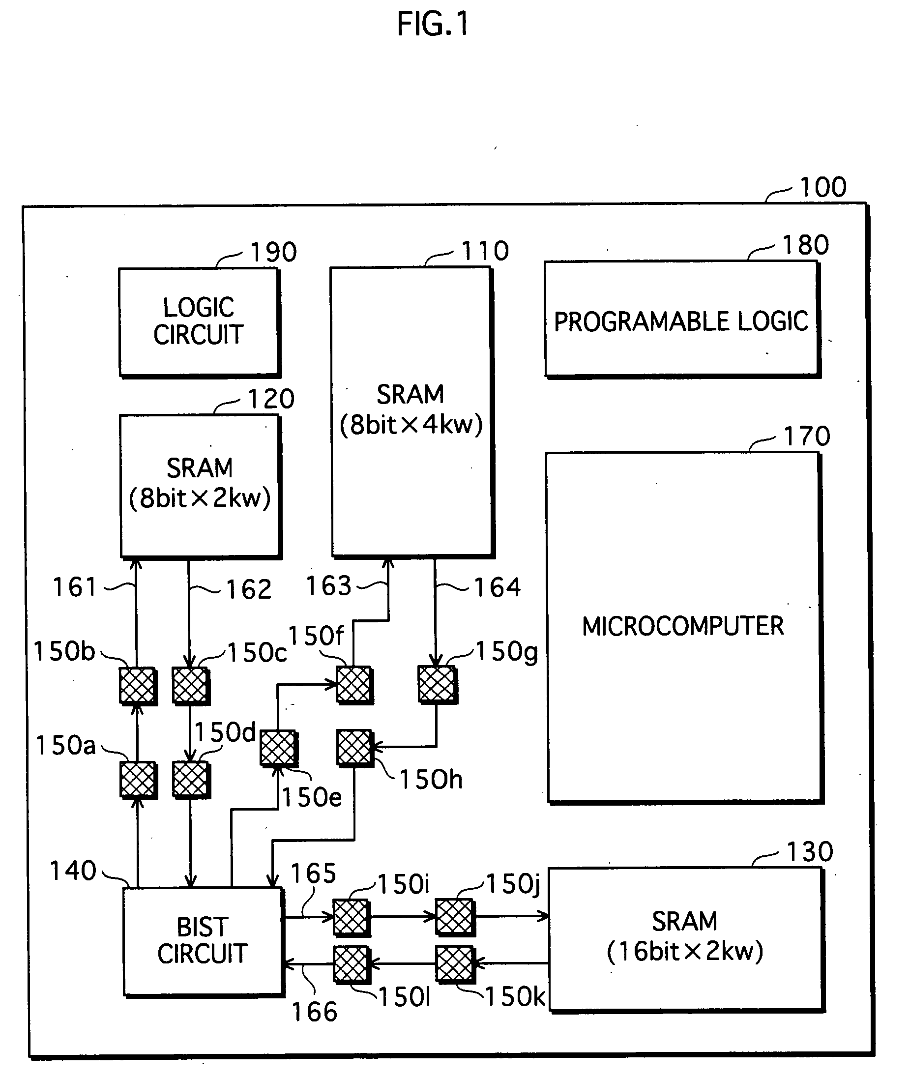
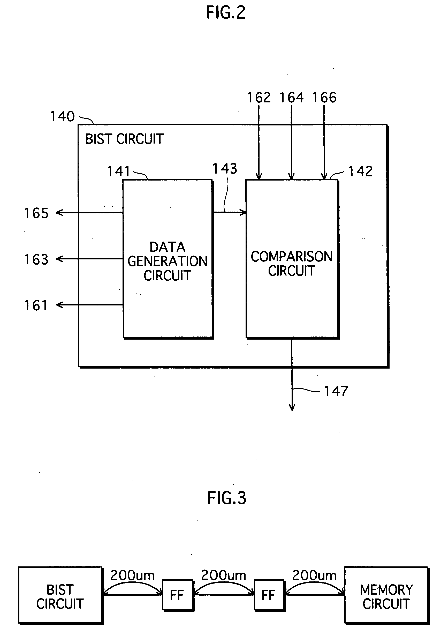
[0038]FIG. 1 shows a layout of an LSI 100 according to the present invention.

[0039]The LSI 100 is a system LSI that includes circuit blocks formed on a semiconductor substrate, namely memories 110, 120 and 130, a BIST circuit 140, registers 150a-150l, a microcomputer 170, a programmable logic circuit 180 and a-logic circuit 190. Note that the LSI 100 may include other circuits in addition to the circuits mentioned above.

[0040]The memory BIST, which is the subject matter of the present invention, is performed on the memories 110, 120 and 130. The memory 110 is an 8-bit×4K-word memory circuit. The memory 120 is an 8-bit×2K-word memory circuit. The memory 130 is a 16-bit×2K-word memory circuit. In the memory BIST, each memory circuit writes test data at a specified address upon receiving a test vector, and reads test data at a specified address upon receiving a read command. Note that one clock cycle (10 ns) is required for each memory circuit to perform each of a write access for writ...

second embodiment

[0069]The second embodiment explains a structure that further reduces the circuit area relating to the BIST.

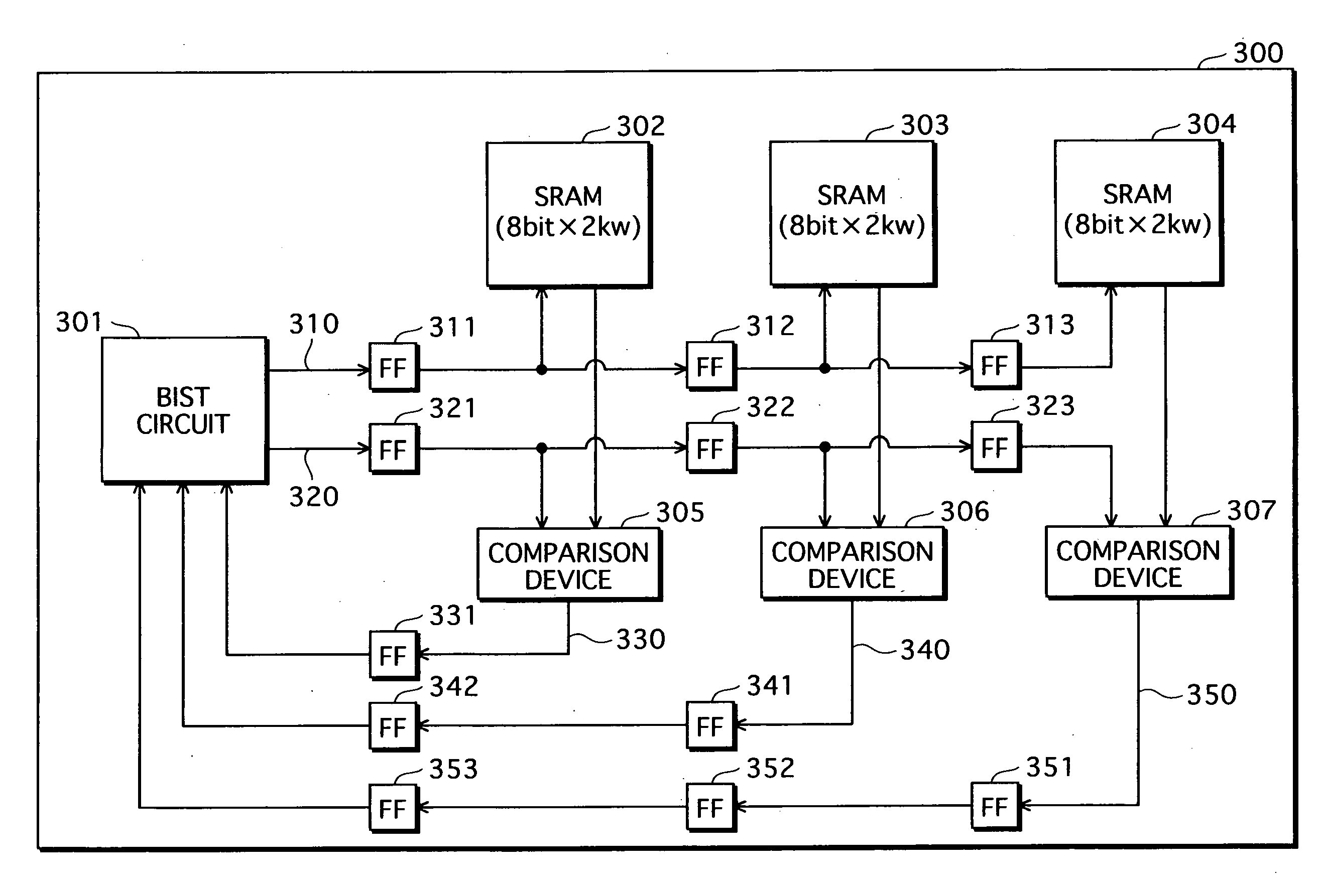
[0070]FIG. 7 shows a structure relating to the BIST in an LSI 300 according to the second embodiment.

[0071]The LSI 300 includes, in addition to a BIST circuit 301 and memories 302, 303 and 304 as targets of the BIST, circuit blocks that are not illustrated, such as a microcomputer, dedicated hardware, and a programmable logic circuit.

[0072]The memories 302, 303 and 304 are memory circuits that are the same as the memories 101, 102 and 103 shown in FIG. 1, and are targets of the BIST test. Each memory circuit outputs a read data to a comparison device corresponding to the memory circuit.

[0073]In the same manner as the data generation unit 141, the BIST circuit 301 has functions of generating and outputting a test vector and a read command, outputting a random number as a comparison data, which has been used as test data in the test vector, and acquiring the comparison results o...

third embodiment

[0084]FIG. 9 shows a structure relating to the BIST in an LSI 500 according to the third embodiment.

[0085]The difference from the LSI 300 shown in FIG. 7 is that the outputs from the comparison devices 305, 306 and 307 in the LSI 500 are connected together as a serial chain.

[0086]As described above, upon receiving the read data of the corresponding memory circuit and the comparison data, each of the comparison devices 305, 306 and 307 compares whether the read data and the comparison data are identical, and outputs the comparison result. Specifically, if the pieces of data are identical, the comparison device outputs “1”, and if not, the comparison device outputs “0”.

[0087]The output from the comparison device 307 is input to a register 361, and the output from the register 361 is input to a logic circuit 365. The output from the comparison device 306 is also input to the logic circuit 364. The logic circuit 364 outputs logical multiplication of the input value. Accordingly, the log...


PUM


Abstract

A semiconductor integrated circuit comprising a plurality of memory circuits; a BSIT circuit 140 operable to output test vectors; and one or more register circuit(s) 150 each allocated on a signal line that transmits test vectors output by the BIST circuit 140 to any of the memory circuits, and operable to sequentially transfer the test vectors to an adjoining macro cell in accordance with the clock signals.

Description

BACKGROUND OF THE INVENTION[0001](1) Field of the Invention[0002]The present invention relates to a BIST (Built-in Self Test) for a semiconductor integrated circuit, and particularly to a technique to test an SRAM at high speed by the BIST.[0003](2) Description of the Related Art[0004]In recent years, a high-integration technique, such as a SoC by which a plurality of processors, a programmable logic circuit, dedicated hardware, a plurality of memories and so on are mounted, has been put into practical use. Due to such high integration, the number of external input / output terminals is comparatively small for its circuit size, and it is difficult to conduct a sufficient test for the semiconductor integrated circuit from outside. Therefore, to test the quality of memory circuits incorporated in the semiconductor integrated circuit, a BIST which uses only the circuits incorporated in the semiconductor integrated circuit is often applied.[0005]However, it is necessary for the BIST to pr...

Claims


Application Information

Patent Timeline
Patent Type & Authority Applications(United States)
IPC IPC(8): G01R31/317
CPCG11C11/41G11C29/12G11C29/1201G11C2029/0401G11C29/14G11C29/26G11C29/38G11C29/12015
Inventor OKABAYASHI, KAZUHIRO
Owner PANASONIC CORP
Why Eureka
Try Eureka