Test handler

a technology of test handler and test handle, which is applied in the direction of individual semiconductor device testing, packaging goods type, instruments, etc., can solve the problems of affecting the overall speed of production of semiconductor devices and damaging such devices, and achieve the effect of maximising the speed of test handling of semiconductor devices

Inactive Publication Date: 2000-10-24
ADVANCED AUTOMATION SYST
View PDF4 Cites 14 Cited by
  • Summary
  • Abstract
  • Description
  • Claims
  • Application Information

AI Technical Summary

Benefits of technology

It is an object of the present invention to maximise the speed of test handling of semiconductor devices without affecting the physical integrity of such devices.
It is another object of the present invention to improve the overall speed of test handling of semiconductor devices by modularising key components of the test handler so that minimum down time occurs during tooling change.
It is yet another object of the present invention to minimise the tooling down time of a test handler by incorporating a quick change plate in the pick and place assembly.
The present invention is a test handler for picking up semiconductor devices from a conveying system and placing them at testing positions and returning the tested devices to the conveying system simultaneously. The basic apparatus has two concentric shafts each connected at one end to a cam following assembly and at the other end to a pick and place arm. The assembly has a block with a centre bore for accommodating transversely a ball screw and a longitudinal channel for receiving a lever cum cam follower subassembly connected to one end of the concentric shafts. The cam follower assembly and the concentric shafts translate the rotational movement of the ball screw into radial movement of the pick and place arms between the conveying system and the test rig. Another pick and insertion assembly associated detachably with the pick and place arms alternately picks up semiconductor devices and places them in position for testing. At the same time, tested devices are returned by the pick and insertion assembly to the conveying system in the same cycle. Each of the pick and place arm features a quick change plate for accommodating a variety of semiconductor device sizes. As such, the present invention handles the testing of semiconductors efficiently and modularly.

Problems solved by technology

Such testing not only poses a bottleneck in the overall speed of production of semiconductor devices but also is a source for damaging such devices if the transfer of semiconductor devices to and forth the testing position is not handled properly.

Method used


Image

  • Test handler
  • Test handler
  • Test handler

Examples


Embodiment Construction

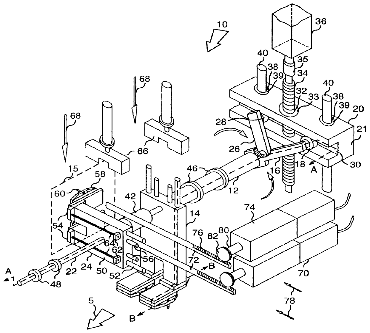
The present invention is an apparatus for test handling semiconductor devices in a testing position. In the following description, numerous specific details are set forth such as pick and place assembly, shafts and ball screw, etc. in order to provide a thorough understanding of the present invention. It will be obvious to one skilled in the art that the present invention may be practiced without these specific details. In other instances, well-known parts such as the chassis of a testing chamber and supporting fixtures are not shown in order not to obscure the present invention.

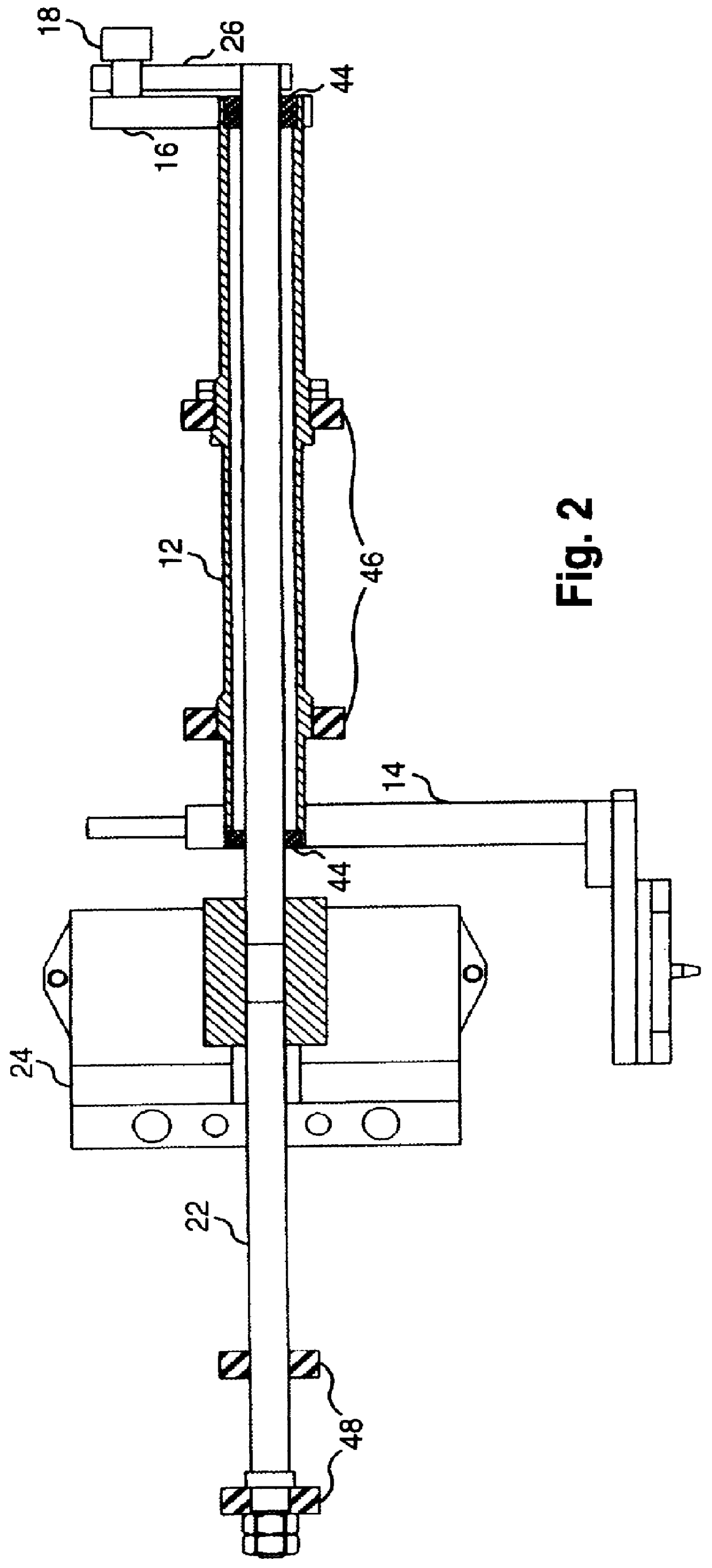
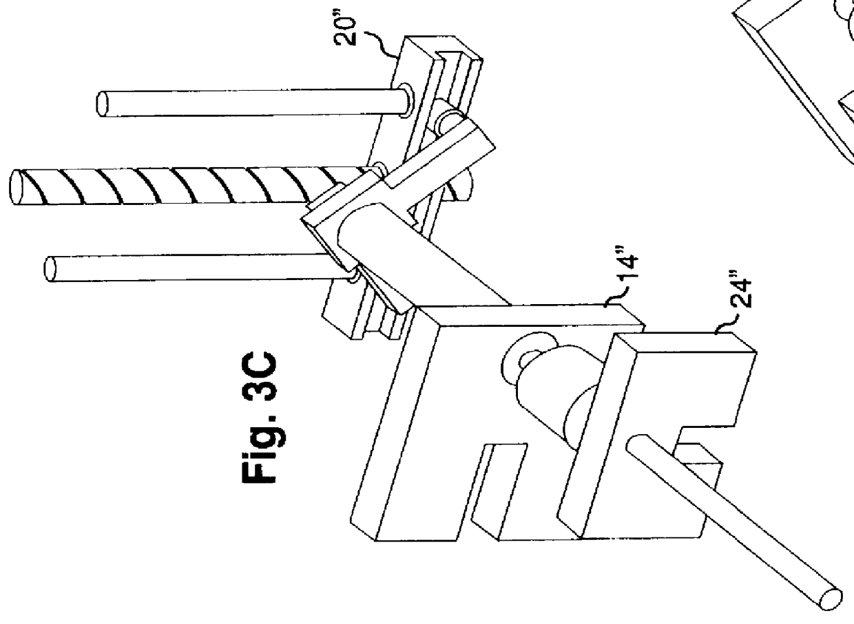
FIG. 1 is an elevational and perspective view of a basic embodiment of a test handler 10 of the present invention. The test handler 10 comprises concentric shafts 12 and 22, pick and place assemblies 14 and 24 coupled to one end of shafts 12 and 22, levers 16 and 26 coupled to the other end of shafts 12 and 22, cam followers 18 and 28 fitted onto the free ends of levers 16 and 26 and preferably seated in a c...


PUM


Abstract

A test handler for picking up semiconductor devices from a conveying system and placing them at testing positions and returning the tested devices to the conveying system efficiently and modularly is shown. The basic apparatus has two concentric shafts each connected at one end to a cam following assembly and at the other end to a pick and place arm. The assembly has a block with a center bore for accommodating a ball screw and a longitudinal channel for receiving a lever cum cam follower subassembly connected to one end of the concentric shafts. The cam follower assembly and the concentric shafts translate the rotational movement of the ball screw into radial movement of the pick and place arms between the conveying system and the test rig. Another pick and insertion assembly associated detachably with the pick and place arms alternately picks up semiconductor devices from the conveying system and places them in position for testing. At the same time, tested devices are returned by the pick and insertion assembly to conveying system in the same cycle. Each of the pick and place arm features a quick change plate for accommodating a variety of semiconductor device sizes. As such, the present invention handles the testing of semiconductors efficiently and modularly.

Description

The present invention relates to a quality control system for testing semiconductor devices. In particular, the present invention pertains to an apparatus for transferring semiconductor devices from a conveying system, placing them into a testing position for testing, and returning the tested devices to the conveying system efficiently and modularly.Quality control is an important stage in the mass production of semiconductor devices. By semiconductor devices, the present invention refers to not only semiconductor chips but also printed circuit boards. However, known methods of meeting quality control of the outputs from semiconductor device production lines require electrical signals to be send to leads of semiconductor devices and response measured therefrom before further packaging of such devices occurs. Such testing not only poses a bottleneck in the overall speed of production of semiconductor devices but also is a source for damaging such devices if the transfer of semiconduc...

Claims


Application Information

Patent Timeline
Patent Type & Authority Patents(United States)
IPC IPC(8): G01R31/01
CPCG01R31/01
Inventor HO, WENG WAHNG, CHILL KWAI
Owner ADVANCED AUTOMATION SYST
Why Eureka
Try Eureka