Monitoring system comprising infrared thermopile detector

a monitoring system and detector technology, applied in the direction of optical radiation measurement, work transfer apparatus, instruments, etc., can solve the problems of loss of radiation intensity, risk of total system failure, cost and complexity of spectrometer apparatus, etc., to reduce the amount of ir radiation transmitted and reduce particle deposi

Inactive Publication Date: 2009-02-12
ADVANCED TECH MATERIALS INC
View PDF44 Cites 9 Cited by
  • Summary
  • Abstract
  • Description
  • Claims
  • Application Information

AI Technical Summary

Benefits of technology

[0013]In one embodiment, infrared (IR) radiation in a system according to the present invention is transmitted along a transmission path that is substantially linear, while both the infrared radiation source and the thermopile detector are aligned along the transmission path of said infrared radiation. The linear transmission path for the IR radiation minimizes reflection and refraction of such IR radiation and therefore significantly reduces loss of radiation intensity during transmission. Such linear transmission path is made available by the integration of the thermopile detector, which comprises one or more radiation filters for selectively transmitting the IR radiation of a specific wavelength, therefore eliminating the requirements for monochromating the IR radiation through splitting and grating that are essential to the conventional dispersive and FT-IR spectrometers.
[0014]The loss of IR radiation intensity can also be reduced, either independent from or in addition to the use of linear transmission path, by providing a transmission path with inner surface that is sufficient smooth and / or reflective, which minimizes absorption and dissipation of the IR radiation by such inner surface of the transmission path. Specifically, such inner surface of the transmission path is characterized by a roughness in a range of from about 0.012 μm Ra to about 1.80 μm Ra, preferably from about 0.10 μm Ra to about 0.80 μm Ra, and more preferably from about 0.10 μm Ra to about 0.20 μm Ra. Such inner surface may further be characterized by a reflectivity in a range of from about 70% to about 99%, preferably from about 92% to about 97%.
[0016]When the material is subjected to IR radiation in the sampling region is a process gas, such material may comprise particles or be susceptible to particle formation, resulting in deposition of particles around the IR radiation source or the thermopile detector, which may in turn significantly reduce the amount of IR radiation transmitted therethrough or completely block the transmission path.
[0017]Various embodiments of the present invention can be arranged and constructed to utilize a purge gas for purging the interfacial spaces between the sampling region containing the process gas and the IR radiation source as well as between the sampling region and the thermopile detector. Such purge gas can be passed through porous media into the interfacial spaces, to form a purge gas flow that moves any particle deposits away from the IR radiation source and the thermopile detector into the sampling region. Alternatively, particle deposit may be reduced by providing external thermal energy for heating at least a portion of the IR transmission path, so as to create a thermal gradient or heat flux that hinders the particle access to the internal surface of the transmission path.
[0018]A semiconductor process system according to one embodiment of the present invention may comprise a scrubber unit for abating a semiconductor process effluent from an upstream process unit, with a sampling region arranged near the inlet of such scrubber unit, so as to enable analysis of the effluent before its entry into such the scrubber unit, thereby enabling the scrubber unit to be responsively operated according the composition of the process gas.

Problems solved by technology

The principal drawbacks of the above-described dispersive spectrometers are the loss of radiation intensity due to multiple reflection and refraction, the risk of total system failure due to misalignment of the movable parts, the cost and complexity of the spectrometer apparatus due to the number of optical components (e.g., mirrors, lens, and prism), and the space requirement for accommodating the numerous optical components used.
Such FT-IR spectrometers suffer from similar drawbacks as described hereinabove for the conventional dispersive spectrometers.

Method used


Image

  • Monitoring system comprising infrared thermopile detector
  • Monitoring system comprising infrared thermopile detector
  • Monitoring system comprising infrared thermopile detector

Examples


Embodiment Construction

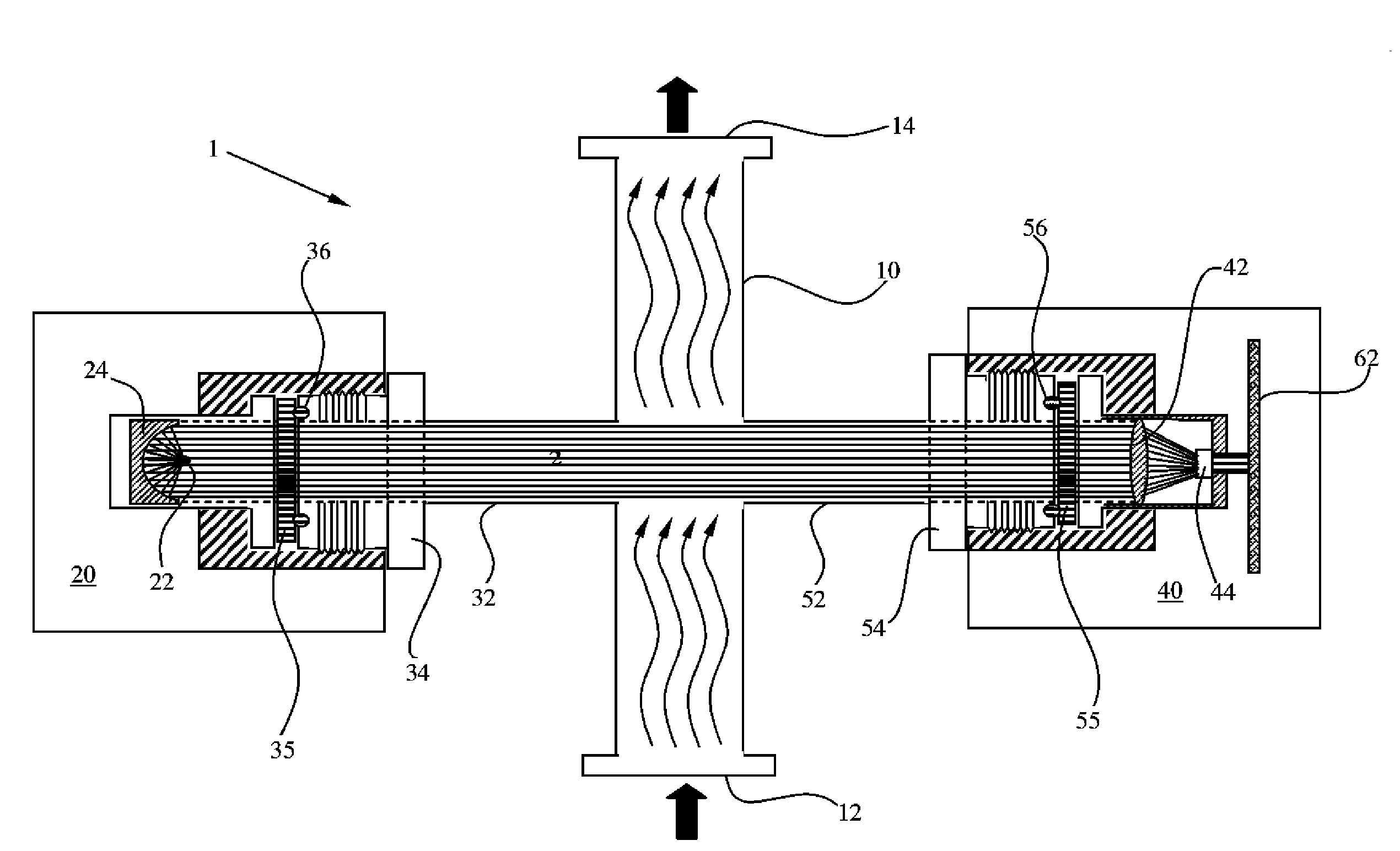
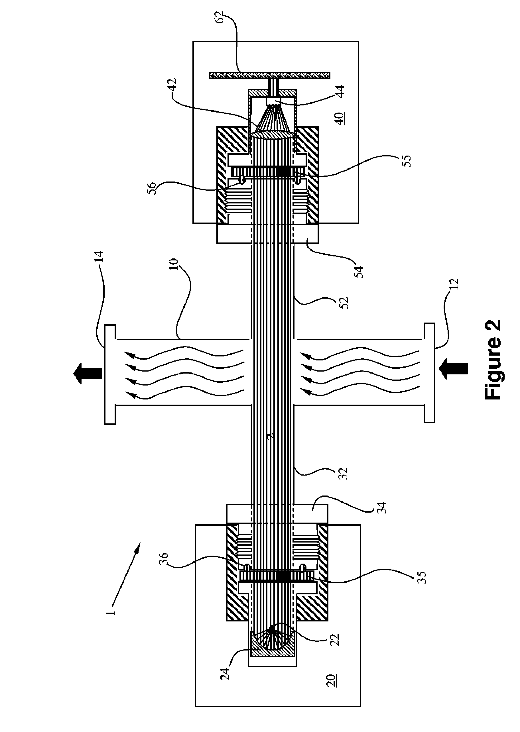
[0027]The present invention provides infrared thermopile detector systems useful for semiconductor process monitoring and control. U.S. patent application Ser. No. 10 / 140,848 filed on May 8, 2002 in the name of Jose I. Arno is incorporated herein by reference in its entirety for all purposes.

[0028]As used herein, the term “semiconductor process” is intended to be broadly construed to include any and all processing and unit operations involved in the manufacture of semiconductor products, as well as all operations involving treatment or processing of materials used in or produced by a semiconductor manufacturing facility, as well as all operations carried out in connection with the semiconductor manufacturing facility not involving active manufacturing (examples include conditioning of process equipment, purging of chemical delivery lines in preparation for operation, etch cleaning of process tool chambers, abatement of toxic or hazardous gases from effluents produced by the semicond...


PUM

PropertyMeasurementUnit
Raaaaaaaaaaa
reflectivityaaaaaaaaaa
Raaaaaaaaaaa

Abstract

The present invention relates to a semiconductor processing system that employs infrared-based thermopile detector for process control, by analyzing a material of interest, based on absorption of infrared light at a characteristic wavelength by such material. In one embodiment, an infrared light beam is transmitted through a linear transmission path from an infrared light source through a sampling region containing material of interest into the thermopile detector. The linear transmission path reduces the risk of signal loss during transmission of the infrared light. The transmission path of the infrared light may comprise a highly smooth and reflective inner surface for minimizing such signal loss during transmission.

Description

CROSS REFERENCE TO RELATED APPLICATIONS[0001]This is a continuation of U.S. patent application Ser. No. 11 / 555,094 filed on Oct. 31, 2006, which is a continuation of U.S. patent application Ser. No. 10 / 668,489 filed on Sep. 23, 2003 and subsequently issued as U.S. Pat. No. 7,129,519, which is a continuation-in-part of U.S. patent application Ser. No. 10 / 623,244 filed on Jul. 18, 2003 and subsequently issued as U.S. Pat. No. 7,011,614, which is a divisional of U.S. patent application Ser. No. 10 / 140,848 filed on May 8, 2002 and subsequently issued as U.S. Pat. No. 6,617,175. Each of the foregoing patents and patent applications is hereby incorporated by reference as if set forth fully herein.FIELD OF THE INVENTION[0002]This invention relates to infrared thermopile monitoring systems for semiconductor process monitoring and control.DESCRIPTION OF THE RELATED ART[0003]Most infrared energy-absorbing molecules absorb infrared radiation at discrete energy levels, so that when a gas, liqui...

Claims


Application Information

Patent Timeline
Patent Type & Authority Applications(United States)
IPC IPC(8): G01J5/02G01N21/35C23C16/52H01L21/00H01L21/205
CPCG01J5/0007G01J5/0014G01J5/025Y10T483/16G01N21/3504H01L21/67253G01J5/12H01L22/00
Inventor ARNO, JOSE I.
Owner ADVANCED TECH MATERIALS INC
Why Eureka
Try Eureka