Integrated circuit system employing a condensation process

a technology of integrated circuits and condensation processes, which is applied in the field of integrated circuit systems, can solve the problems of long eluded skilled in the art, and the failure of conventional processes to maximize the strain inducing effect, and achieve the effect of reducing the number of circuits

Active Publication Date: 2009-02-12
CHARTERED SEMICONDUCTOR MANUFACTURING
View PDF4 Cites 56 Cited by
  • Summary
  • Abstract
  • Description
  • Claims
  • Application Information

AI Technical Summary

Problems solved by technology

Unfortunately, these conventional processes fail to maximize the strain inducing effect that different concentration levels for the source/drain extensions and the source/drain regions can have on the...

Method used


Image

  • Integrated circuit system employing a condensation process
  • Integrated circuit system employing a condensation process
  • Integrated circuit system employing a condensation process

Examples


Embodiment Construction

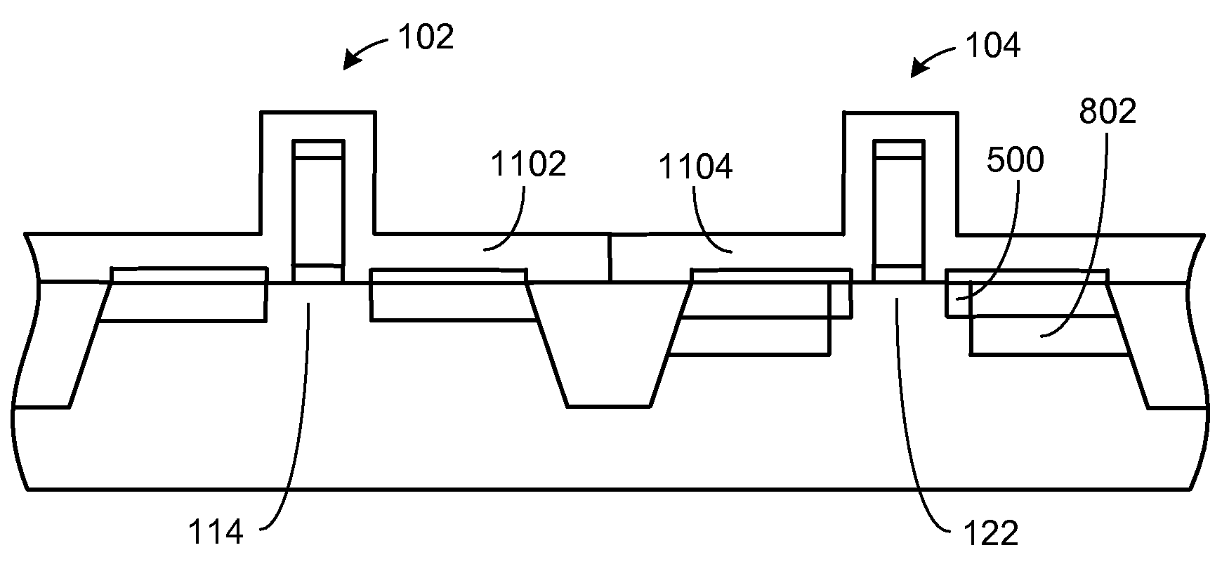
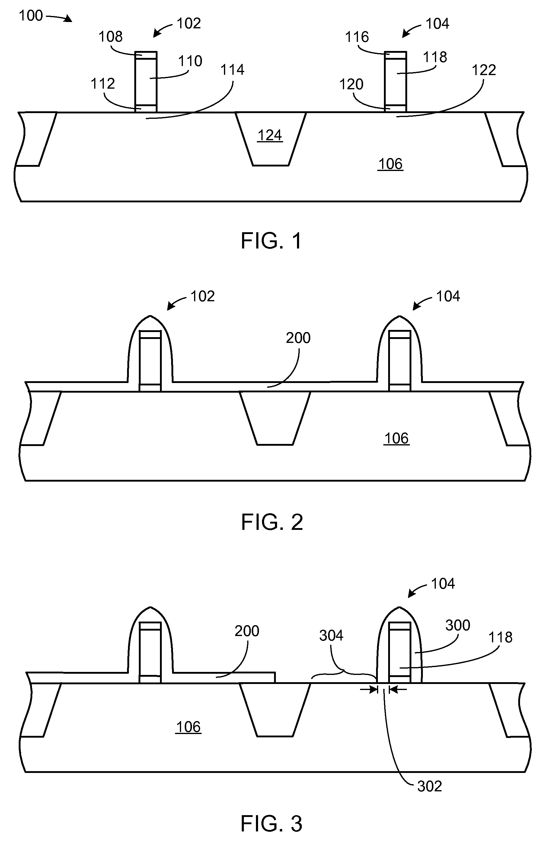
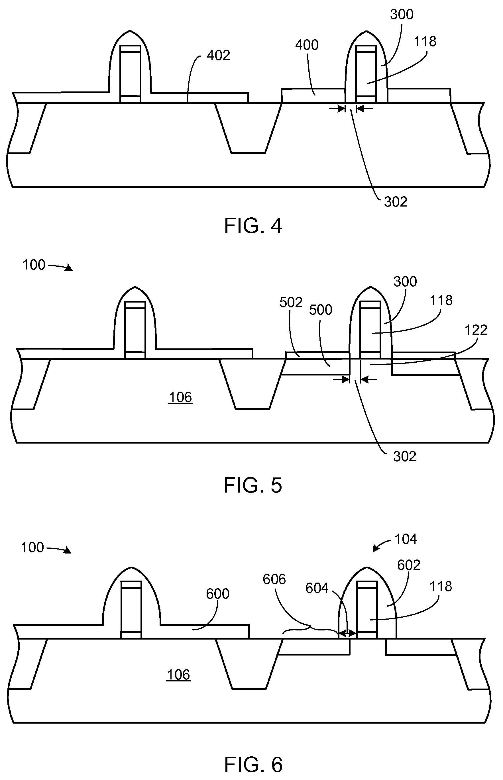
[0032]The following embodiments are described in sufficient detail to enable those skilled in the art to make and use the invention. It is to be understood that other embodiments would be evident based on the present disclosure, and that process or mechanical changes may be made without departing from the scope of the present invention.

[0033]In the following description, numerous specific details are given to provide a thorough understanding of the invention. However, it will be apparent that the invention may be practiced without these specific details. In order to avoid obscuring the present invention, some well-known circuits, system configurations, and process steps are not disclosed in detail.

[0034]Likewise, the drawings showing embodiments of the system are semi-diagrammatic and not to scale and, particularly, some of the dimensions are for the clarity of presentation and are shown exaggerated in the drawing FIGs. Additionally, where multiple embodiments are disclosed and desc...


PUM


Abstract

An integrated circuit system that includes: providing a PFET device including a PFET gate and a PFET gate dielectric; forming a source/drain extension from a first epitaxial layer aligned to a first PFET gate sidewall spacer; and forming a source/drain from a second epitaxial layer aligned to a second PFET gate sidewall spacer.

Description

TECHNICAL FIELD[0001]The present invention relates generally to integrated circuits, and more particularly to an integrated circuit system employing a condensation process.BACKGROUND ART[0002]Integrated circuits find application in many of today's consumer electronics, such as cellphones, video cameras, portable music players, printers, computers, etc. Integrated circuits may include a combination of active devices, passive devices and their interconnections.[0003]A common active device within an integrated circuit is the metal-oxide-semiconductor field-effect transistor (MOSFET), which is commonly referred to as a field-effect transistor (FET). A MOSFET generally includes a semiconductor substrate, having a source, a drain, and a channel located between the source and drain. A gate stack including a conductive material (i.e.—a gate) and an oxide layer (i.e.—a gate oxide) are typically located above the channel. During operation, an inversion layer forms a conducting bridge or “chan...

Claims


Application Information

Patent Timeline
IPC IPC(8): H01L29/778H01L21/336
CPCH01L21/823807H01L21/823814H01L29/7848H01L29/6653H01L29/66636H01L21/823864
Inventor TEO, LEE WEECHONG, YUNG FUQUEK, ELGIN KIOK BOONECHAN, ALAIN
Owner CHARTERED SEMICONDUCTOR MANUFACTURING
Why Eureka
Try Eureka