
Patsnap Eureka
For R&D, Patsnap Eureka makes reading and utilizing patents & technical documents easy.
Patsnap Eureka AIR
Designed for self-driven R&D workflows. Generate viable solutions, solve complex R&D challenges, empower your innovation with AI.

Patsnap Eureka Materials
Designed for material experts only. Revolutionize your material R&D, from search, analyze, to developing new materials.

TechResearch
Generate reliable direction feasibility study reports for your R&D in just a few steps.

TechSeek
Discover and master advanced knowledge NOW. Basics, ideas, possibilities, all at once.

TechMind
As an expert in R&D Theories, TechMind can generates customized viable solutions instantly.

TechRisk
Analyze your overall solution with one click, know your potential R&D risks in advance.

TechMonitor
Get weekly tech updates, stay abreast of the latest tech innovations and key insights.
Heat slug and semiconductor package
a technology of heat slugs and semiconductors, applied in semiconductor/solid-state device details, cooling/ventilation/heating modifications, semiconductor devices, etc., can solve the problems of increasing the complexity of designing and manufacturing the substrate, and the b>97/b> of adhesives is not usually cured immediately
- Summary
- Abstract
- Description
- Claims
- Application Information
AI Technical Summary
Benefits of technology
Problems solved by technology
Method used
Image

Examples
Embodiment Construction
[0020]The foregoing, as well as additional objects, features and advantages of the invention will be more readily apparent from the following detailed description, which proceeds with reference to the accompanying drawings.
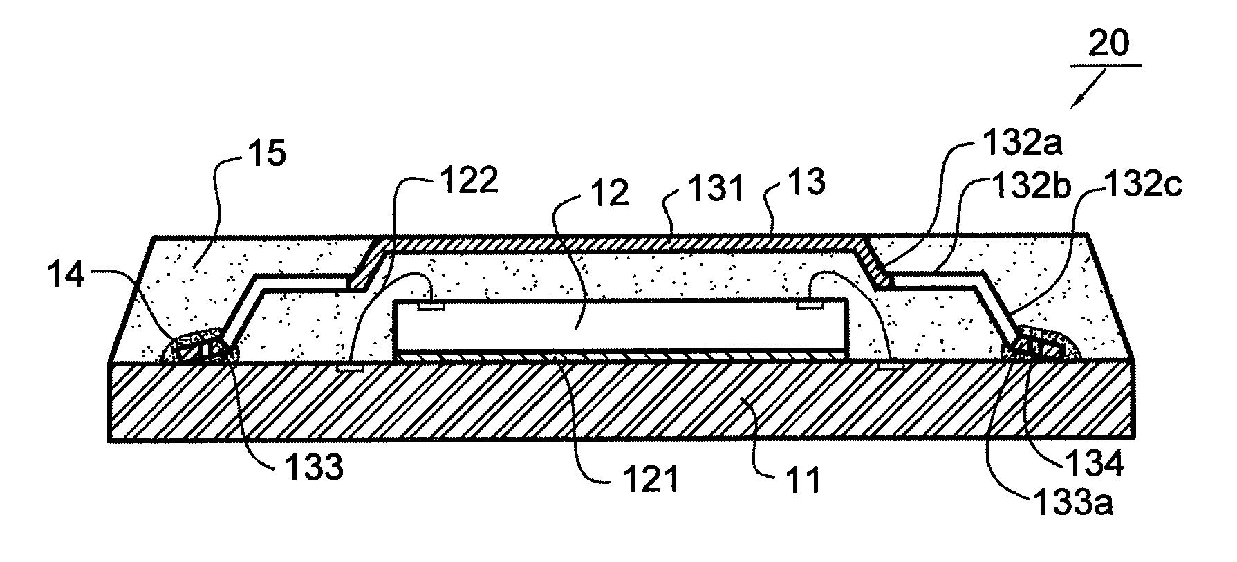
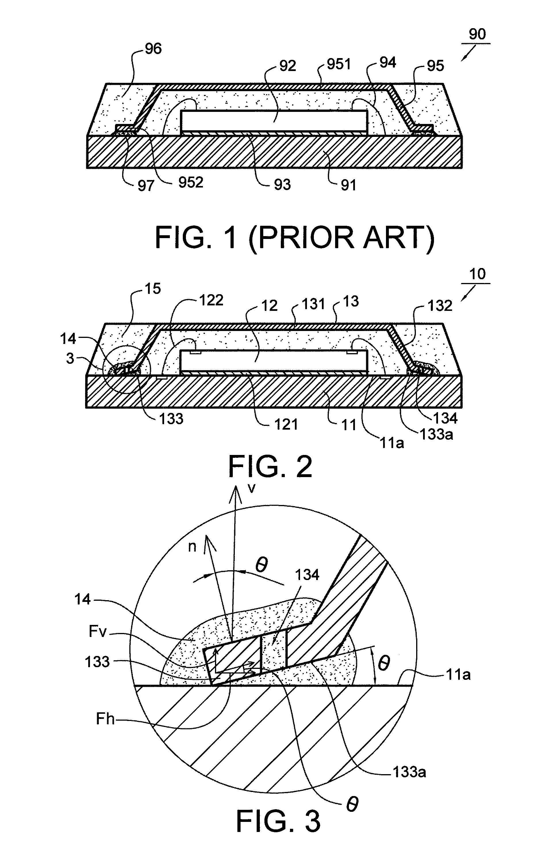
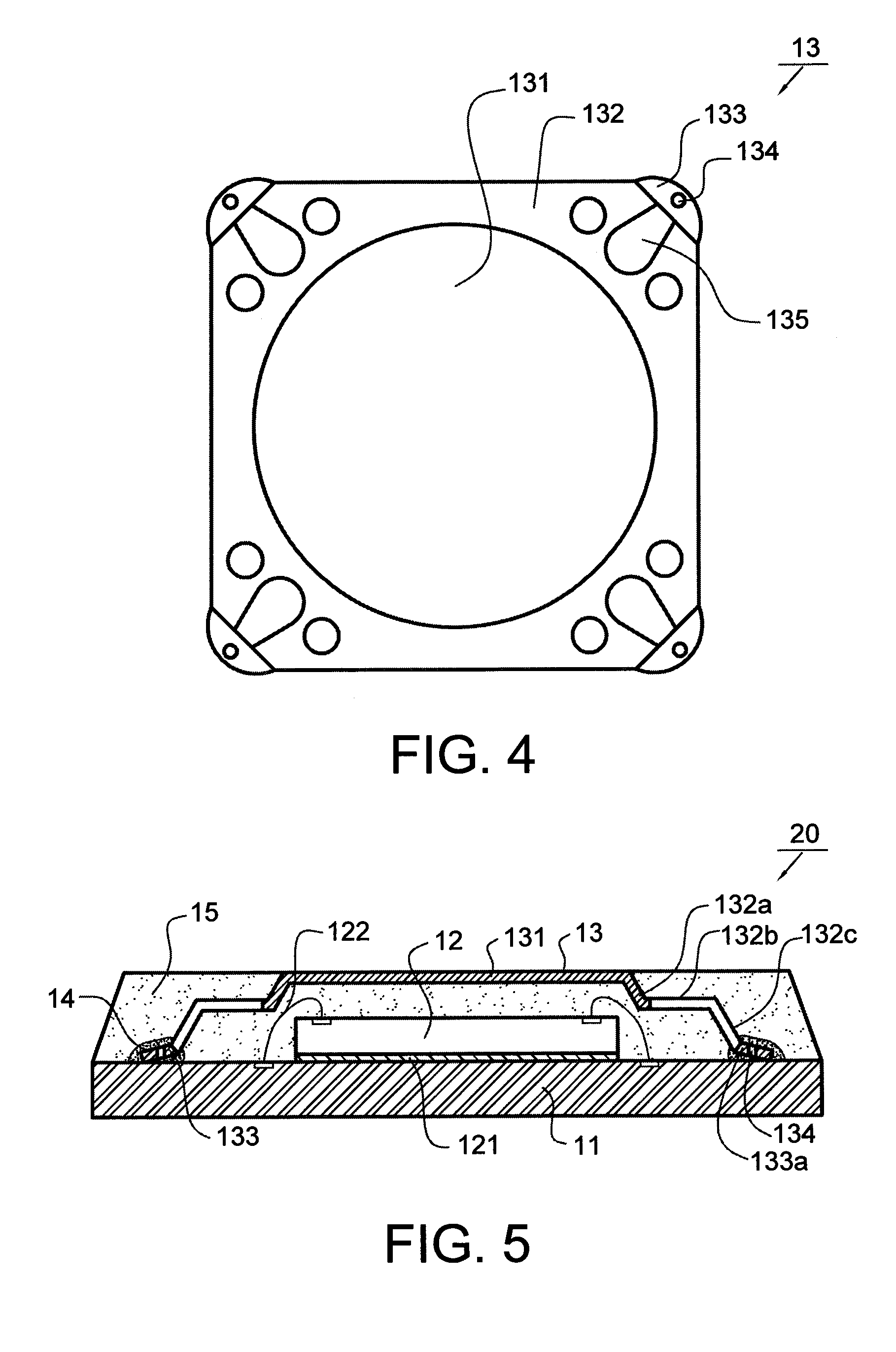
[0021]Referring to FIG. 2, it illustrates a cross-sectional view of the semiconductor package 10 according to the present invention. The semiconductor package 10 includes a chip carrier 11, a chip 12, a heat slug 13, an adhesive 14 and a sealant 15. The chip carrier 11 can be such as a substrate and has an upper surface 11a for carrying the chip 12 and heat slug 13. The upper surface 11a of the chip carrier 11 is provided with a plurality of bonding pads (not labeled in the figure) and a wiring trace (not shown in the figure).
[0022]The chip 12 is bonded to the chip carrier 11 through a die adhesive 121. The active surface of the chip 12 is provided with a plurality of bonding pads (not labeled in the figure). A plurality of bonding wires 122 is used to electricall...
PUM
 Abstract
Description
Claims
Application Information
 - R&D Engineer
- R&D Manager
- IP Professional
- Industry Leading Data Capabilities
- Powerful AI technology
- Patent DNA Extraction
Browse by: Latest US Patents, China's latest patents, Technical Efficacy Thesaurus, Application Domain, Technology Topic, Popular Technical Reports.
© 2024 PatSnap. All rights reserved.Legal|Privacy policy|Modern Slavery Act Transparency Statement|Sitemap|About US| Contact US: help@patsnap.com