Organic light emitting display apparatus and method of manufacturing the same

a technology of light-emitting display and organic light-emitting display, which is applied in the manufacture of electrode systems, electric discharge tubes/lamps, discharge tubes luminescnet screens, etc., can solve the problems of complicated manufacturing process costs, and high manufacturing process costs, so as to simplify the patterning process and reduce the manufacturing process costs

Active Publication Date: 2009-02-12
SAMSUNG DISPLAY CO LTD
View PDF2 Cites 42 Cited by
  • Summary
  • Abstract
  • Description
  • Claims
  • Application Information

AI Technical Summary

Benefits of technology

[0009]Aspects of the present invention provide an organic light emitting display apparatus in which a patterning process using a mask is simplified and costs for the manufacturing process are reduced and a method of manufacturing the organic light emitting display apparatus.

Problems solved by technology

However, since two masks are used to pattern the pixel defining layer 15 and the spacer 16 in a conventional organic light emitting display apparatus, the manufacturing process is complicated, and thus the costs for the manufacturing process are high.
Alternatively, the use of a half-tone mask including a semi-penetrating unit in addition to a light blocking unit and a light penetrating unit may simplify the manufacturing process, but this technique may also lead to high costs for the manufacturing process even though only one mask is used, since a half-tone mask is more expensive than a conventional mask.

Method used


Image

  • Organic light emitting display apparatus and method of manufacturing the same
  • Organic light emitting display apparatus and method of manufacturing the same
  • Organic light emitting display apparatus and method of manufacturing the same

Examples


Embodiment Construction

[0033]Reference will now be made in detail to the present embodiments of the present invention, examples of which are illustrated in the accompanying drawings, wherein like reference numerals refer to the like elements throughout. The embodiments are described below in order to explain the present invention by referring to the figures.

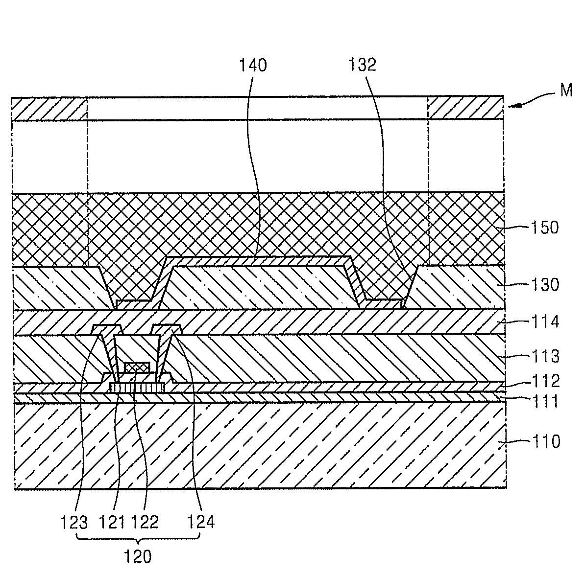
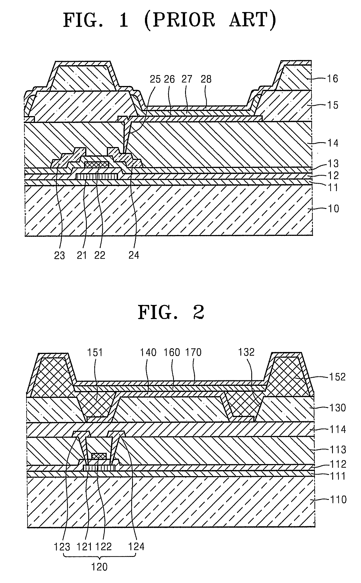
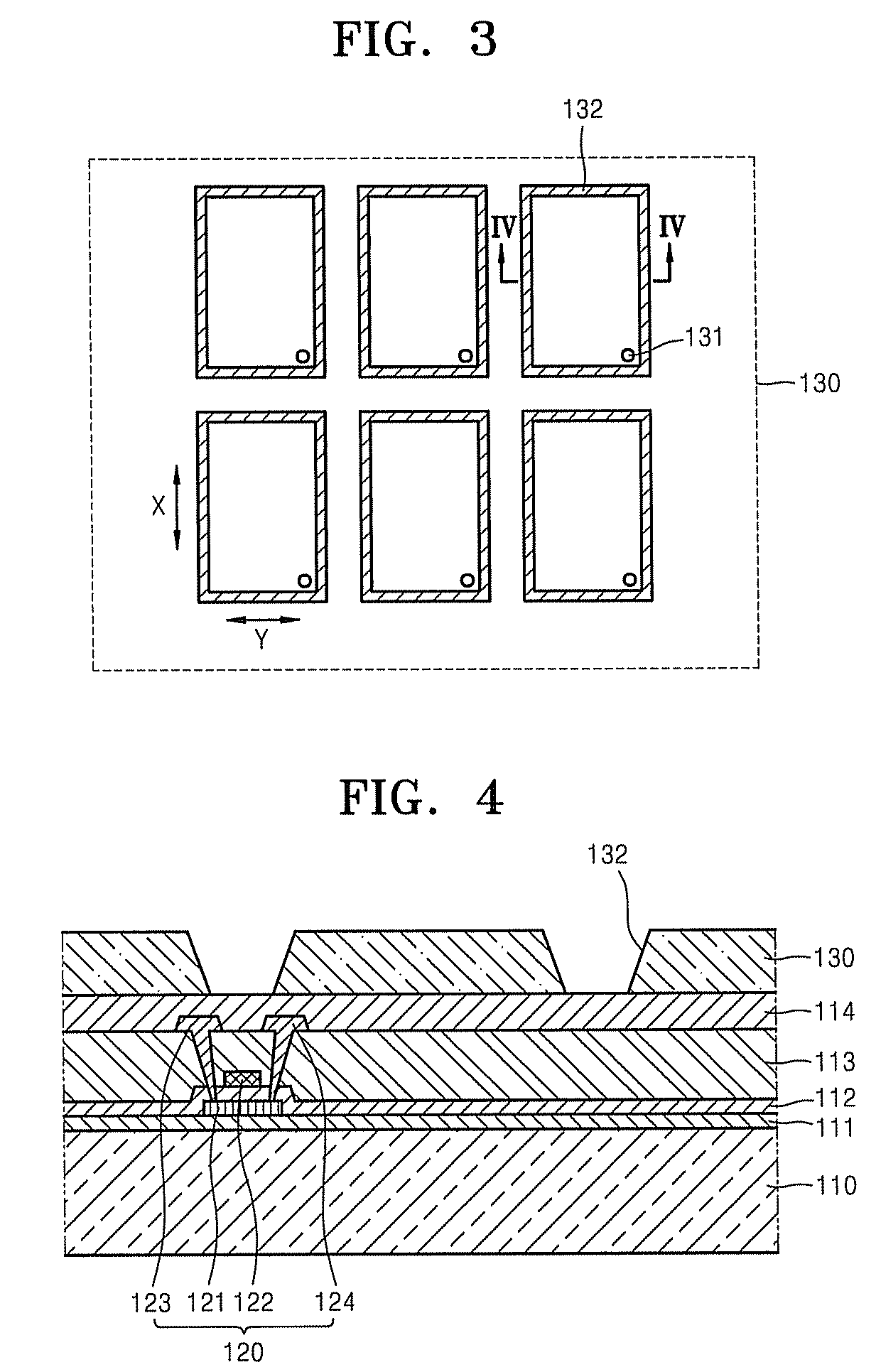
[0034]FIG. 2 is a schematic cross-sectional view of an organic light emitting display apparatus according to an embodiment of the present invention. FIG. 3 is a plan view and FIGS. 4 through 6 are schematic cross-sectional views showing a process of preparing the organic light emitting display apparatus of FIG. 2.

[0035]Referring to FIG. 2, an organic light emitting display apparatus according to an embodiment of the present invention includes a substrate 110, a buffer layer 111, a gate insulating layer 112, an interlevel dielectric layer 113, a thin film transistor 120, a passivation layer 114, a planarization layer 130, a pixel electrode 140, a pixel ...


PUM


Abstract

An organic light emitting display apparatus including: a substrate; a thin film transistor formed on the substrate; a planarization layer formed on the substrate to cover the thin film transistor and comprising a closed-loop groove; a pixel electrode that contacts the thin film transistor and is formed on the planarization layer; a pixel defining layer formed to fill the closed-loop groove; a spacer formed on the planarization layer and disposed outside the pixel electrode; an organic light emitting layer formed on the pixel electrode; and an opposite electrode covering the organic light emitting layer.

Description

CROSS-REFERENCE TO RELATED APPLICATION[0001]This application claims the benefit of Korean Application No. 2007-80332, filed Aug. 9, 2007, in the Korean Intellectual Property Office, the disclosure of which is incorporated herein by reference.BACKGROUND OF THE INVENTION[0002]1. Field of the Invention[0003]Aspects of the present invention relate to an organic light emitting display apparatus and a method of manufacturing the organic light emitting display apparatus. More particularly, aspects of the present invention relate to an organic light emitting display apparatus in which a manufacturing process is simplified and costs for the manufacturing process are reduced and a method of manufacturing the organic light emitting display apparatus.[0004]2. Description of the Related Art[0005]Organic light emitting display apparatuses are self-emitting display devices having an organic light emitting layer between a pixel electrode and an opposite electrode. In such organic light emitting dis...

Claims


Application Information

Patent Timeline
Patent Type & Authority Applications(United States)
IPC IPC(8): H01J1/62H01J9/00
CPCH01L27/3246H01L51/525H01L27/3258H10K59/124H10K59/122H10K50/8428H05B33/22H05B33/26
Inventor JUN, WOO-SIKKANG, CHUL-KYU
Owner SAMSUNG DISPLAY CO LTD
Why Eureka
Try Eureka