Method for manufacturing bonded wafer and outer-peripheral grinding machine of bonded wafer

a technology of bonded wafer and grinding machine, which is applied in the direction of grinding machine, grinding/polishing apparatus, manufacturing tools, etc., can solve the problems of likely chipping or delaminate of the outer peripheral portion of the thinned bond wafer, and achieve high-quality bonded wafer, ensure enough strength, and efficient grinding

Active Publication Date: 2009-02-12
SHIN-ETSU HANDOTAI CO LTD
View PDF9 Cites 22 Cited by
  • Summary
  • Abstract
  • Description
  • Claims
  • Application Information

AI Technical Summary

Benefits of technology

[0043]If the outer-peripheral grinding machine includes a disk-like grind stone in addition to the end mill type one as described above, various types of wafers can be efficiently ground with one outer-peripheral grinding machine such that an orientation flat portion and a notch portion are formed with the end mill type grind stone, and the other portion is formed with the dicer type grind stone, for example.
[0044]As described above, according to the present invention, the outer peripheral portion of the bond wafer is ground to form a groove along the outer peripheral portion in the step of grinding the outer peripheral portion, and the outer edge portion formed outside the groove is left with such a thickness as ensures enough strength. The outer edge portion can be removed together with the groove portion in a subsequent etching step. Thus, chipping or delamination hardly occurs during grinding. Therefore, dimples are rarely formed in a terrace portion upon grinding and etching the outer peripheral portion, and a high-quality bonded wafer can be manufactured with high yield.

Problems solved by technology

In this case, the outer peripheral portion of the thinned bond wafer is likely to chip or delaminate.

Method used


Image

  • Method for manufacturing bonded wafer and outer-peripheral grinding machine of bonded wafer
  • Method for manufacturing bonded wafer and outer-peripheral grinding machine of bonded wafer
  • Method for manufacturing bonded wafer and outer-peripheral grinding machine of bonded wafer

Examples


example 1

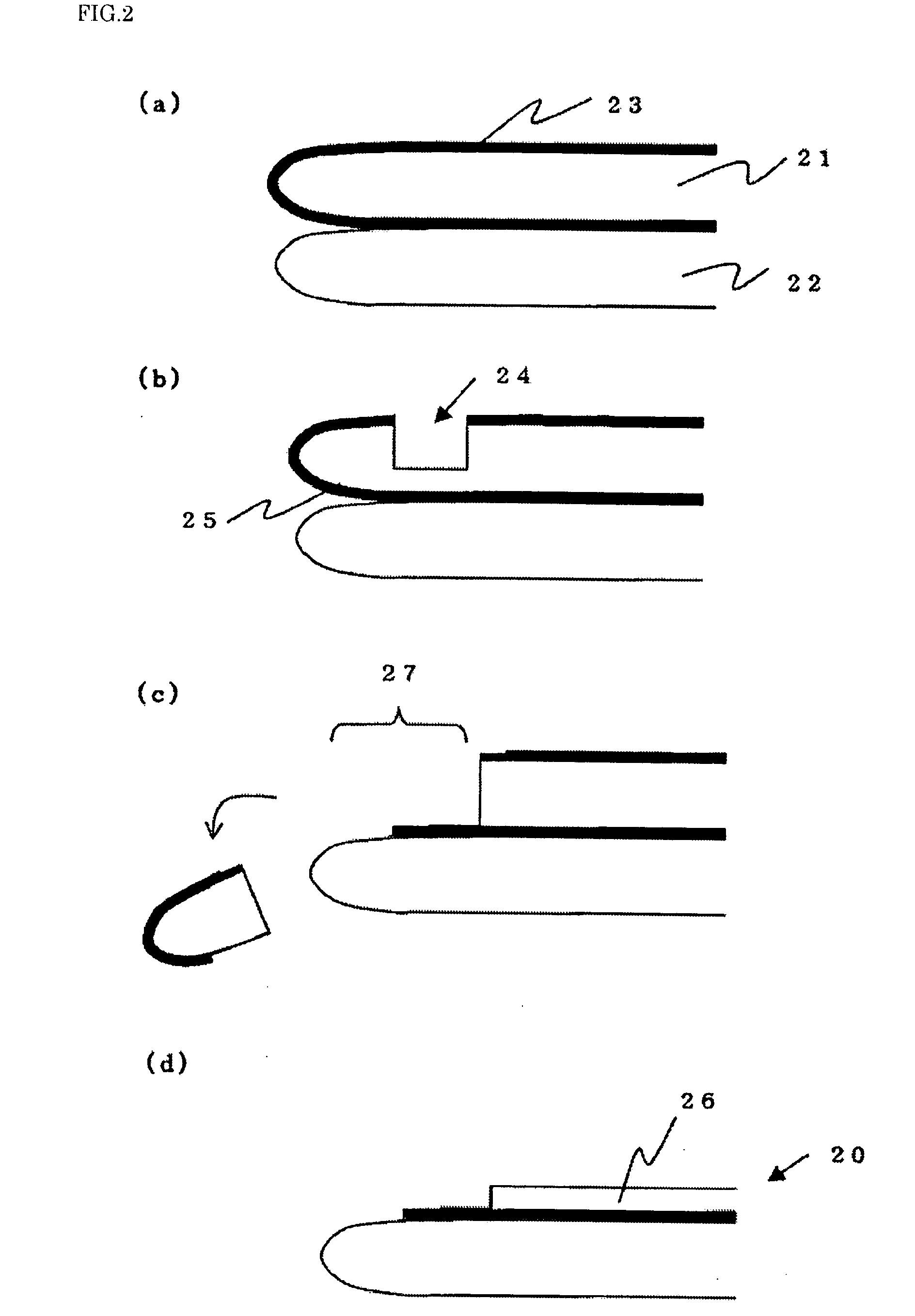
[0081]A bonded wafer was manufactured in accordance with a procedure of FIG. 2.

[0082]First, 10 mirror-polished CZ wafers having the diameter of 150 mm (6 inches), a thickness of 625 microns, a p-type conductivity, and a resistivity of 4 to 6 Ω·cm were prepared and divided into 5 wafers for bond wafers and 5 wafers for base wafers. Among those, the bond wafer 21 was subjected to heat treatment and the oxide film 23 was formed on the surface of the bond wafer.

[0083]Then, the bond wafer 21 having the oxide film 23 formed thereon and the base wafer 22 were bonded together under clean atmosphere and then, subjected to bonding heat treatment at 1200° C. under an oxidizing atmosphere to manufacture 5 bonded wafers in total (see FIG. 2(a)).

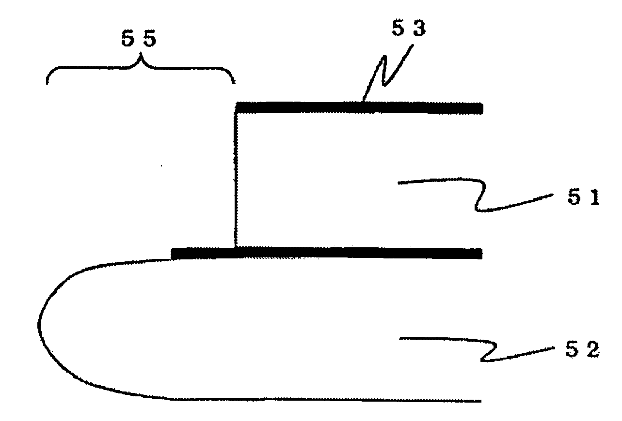
[0084]Next, the bond wafer 21 was ground to form the groove 24 along the outer peripheral portion thereof to form the outer edge portion 25 outside the groove 24 (see FIG. 2(b)).

[0085]At this time, the width of the outer edge portion 25 was set to 500 μm ...


PUM


Abstract

The present invention provides a method for manufacturing a bonded wafer, which includes at least the steps of bonding a bond wafer and a base wafer, grinding an outer peripheral portion of the bonded bond wafer, etching off an unbonded portion of the ground bond wafer, and then reducing a thickness of the bond wafer, wherein, in the step of grinding the outer peripheral portion, the bonded bond wafer is ground so as to form a groove along the outer peripheral portion of the bond wafer to form an outer edge portion outside the groove; and in the subsequent step of etching, the outer edge portion is removed together with the groove portion of the bond wafer to form a terrace portion where the base wafer is exposed at the outer peripheral portion of the bonded wafer. Thus, it is possible to provide a method for manufacturing a bonded wafer, which can reduce the number of dimples formed in a terrace portion of a base wafer upon removing an outer peripheral portion of a bonded bond wafer.

Description

TECHNICAL FIELD[0001]The present invention relates to a method for manufacturing a bonded wafer and more specifically, the invention relates to a method for manufacturing a bond wafer comprising grinding an outer peripheral portion of a bonded bond wafer, followed by etching to remove an unbonded portion of the bonded bond wafer. In addition, the present invention relates to an outer-peripheral grinding machine of a bonded wafer, which is used for the method for manufacturing such a bonded wafer.BACKGROUND ART[0002]Bonded wafers prepared by bonding a bond wafer to a base wafer and then reducing the thickness of the wafer used for fabricating device (bond wafer), have been used as a wafer for a high-performance device.[0003]An SOI wafer has been known as one of the bonded wafers. This wafer can be manufactured as follows, for instance. That is, two mirror-polished silicon wafers (bond wafer and base wafer) are prepared, and an oxide film is formed on at least one wafer. Then, these w...

Claims


Application Information

Patent Timeline
Patent Type & Authority Applications(United States)
IPC IPC(8): H01L21/30B24B5/00
CPCH01L21/2007H01L21/76256H01L21/304H01L21/20
Inventor MIYAZAKI, SUSUMUTAKEI, TOKIOOKABE, KEIICHI
Owner SHIN-ETSU HANDOTAI CO LTD
Why Eureka
Try Eureka