Display device

a display device and display screen technology, applied in the field of display devices, can solve the problems of reducing the refractive index, reducing and the touch panel itself increasing the thickness and weight of the entire device or the cost, so as to achieve stable touch panel operation and suppress capacitive coupling

Active Publication Date: 2009-02-19
SHARP KK
View PDF8 Cites 140 Cited by
  • Summary
  • Abstract
  • Description
  • Claims
  • Application Information

AI Technical Summary

Benefits of technology

[0066]According to the invention, a shield electrode for suppressing capacitive coupling is formed between a first transparent electrode for detecting a tou

Problems solved by technology

However, the resistive touch panel, in which the pair of transparent conductive films are disposed to face each other with the airspace interposed therebetween, has a drawback in that the airspace causes difference in refractive index to increase, resulting in a reduction i

Method used


Image

  • Display device
  • Display device
  • Display device

Examples


first embodiment

of the Invention

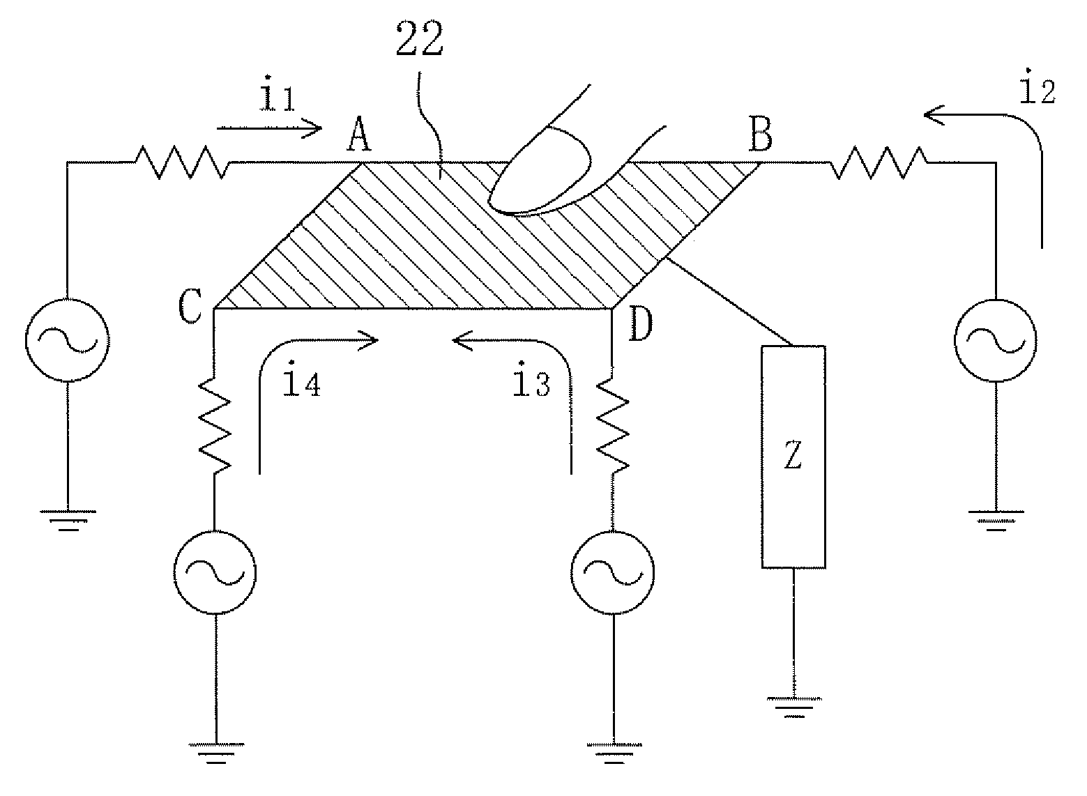
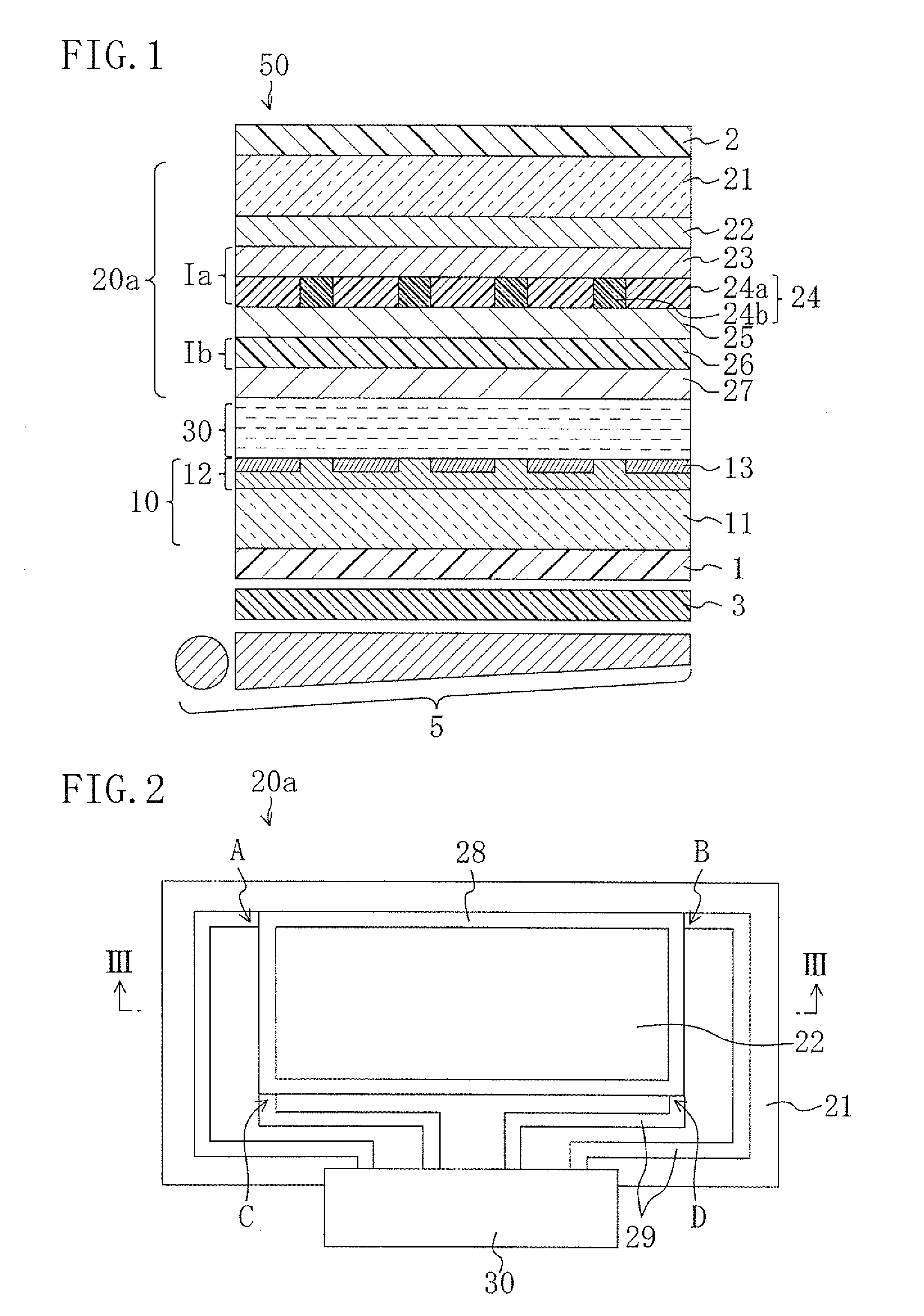
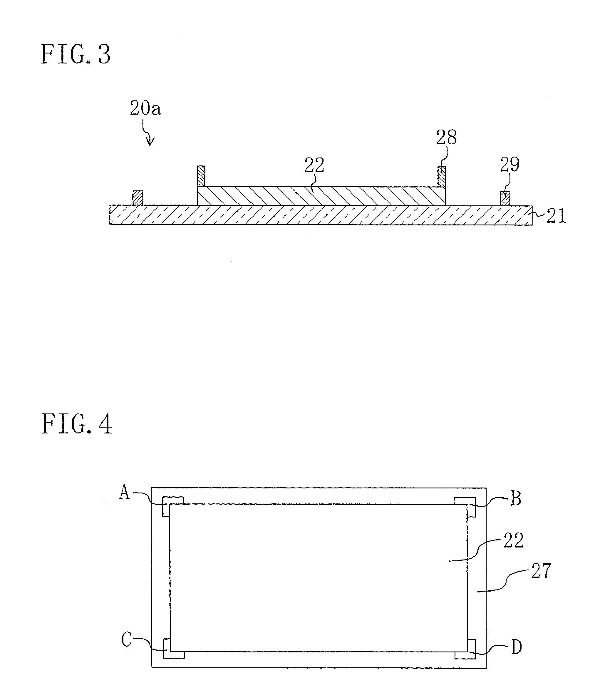
[0093]FIGS. 1 to 6 show a liquid crystal display device according to a first embodiment of the invention. Specifically, FIG. 1 is a schematic cross-sectional view of a liquid crystal display device 50 according to this embodiment. FIG. 2 is a schematic plan view of part of a touch panel 20a included in the liquid crystal display device 50, and FIG. 3 is a schematic cross-sectional view taken along the line III-III in FIG. 2.

[0094]As shown in FIG. 1, the liquid crystal display device 50 includes: an active matrix substrate 10; a touch panel substrate 20a disposed to face the active matrix substrate 10; a liquid crystal layer 30 as a display medium layer interposed between the active matrix substrate 10 and the touch panel substrate 20a; a back light 5 placed under the active matrix substrate 10 with a polarizing plate 1 and a diffusion sheet 3 interposed therebetween; and a polarizing plate 2 formed on the touch panel substrate 20a.

[0095]The active matrix substrate 1...

second embodiment

of the Invention

[0163]FIG. 7 is a schematic cross-sectional view of a touch panel substrate 20b included in a liquid crystal display device according to this embodiment. In the following embodiments, the same members as those shown in FIGS. 1 to 6 are identified by the same reference numerals and detailed description thereof will be omitted herein.

[0164]The liquid crystal display device of this embodiment includes the touch panel substrate 20b in place of the touch panel substrate 20a of the first embodiment.

[0165]In the touch panel substrate 20b, the positional relationship between a color filter layer 24 and a shield electrode 25 is opposite to that in the touch panel substrate 20a of the first embodiment. In the other respects, the configuration of the touch panel substrate 20b is the same as that of the touch panel substrate 20a.

[0166]The touch panel substrate 20b is prepared just by interchanging the process step of forming the color filter layer 24 and the process step of for...

third embodiment

of the Invention

[0169]FIG. 8 is a schematic cross-sectional view of a touch panel substrate 20c included in a liquid crystal display device according to this embodiment.

[0170]The liquid crystal display device of this embodiment includes the touch panel substrate 20c in place of the touch panel substrate 20a of the first embodiment.

[0171]In the touch panel substrate 20c, which is obtained by forming an organic insulating layer 26a between the color filter layer 24 and the shield electrode 25 in the touch panel substrate 20a of the first embodiment, a shield electrode 25 is sandwiched between a pair of organic insulating layers 26a and 26b. In the other respects, the configuration of the touch panel substrate 20c is the same as that of the touch panel substrate 20a.

[0172]In the liquid crystal display device including the touch panel substrate 20c of this embodiment, since the shield electrode 25 is formed between a first transparent electrode 22 and a second transparent electrode 27 ...


PUM


Abstract

A display device includes: a first substrate and a second substrate disposed to face each other; a display medium layer interposed between the first substrate and the second substrate; a plurality of pixel electrodes arranged in a matrix between the first substrate and the display medium layer; a first transparent electrode, interposed between the second substrate and the display medium layer, for detecting a touched location; and a second transparent electrode, interposed between the first transparent electrode and the display medium layer, for receiving a display signal. The display device detects the touched location using a capacitive coupling method and displays an image. A shield electrode for suppressing capacitive coupling is formed between the first transparent electrode and the second transparent electrode.

Description

TECHNICAL FIELD[0001]The present invention relates to display devices, and particularly relates to a display device including a capacitive touch panel.BACKGROUND ART[0002]A touch panel is a device for inputting, with a touch (pressing) of a finger, a stylus, etc., information to an information processing device such as a computer in an interactive manner.[0003]Touch panels are classified by their principle of operation into different types, such as resistive, capacitive, infrared, ultrasonic wave, and electromagnetic induction coupling. Resistive touch panels and capacitive touch panels can be incorporated into display devices, etc., at low cost and are thus widely used in recent years.[0004]A resistive touch panel, which is composed of, for example, a pair of glass substrates disposed to face each other, transparent conductive films provided as resistive films on the entire inner surfaces of the pair of glass substrates, an insulating spacer sandwiched between the pair of glass sub...

Claims


Application Information

Patent Timeline
IPC IPC(8): G06F3/045
CPCG06F3/044G06F3/0412G06F2203/04107G06F3/0444
Inventor TANAKA, SHINYAKATAOKA, YOSHIHARU
Owner SHARP KK
Why Eureka
Try Eureka