Solid state lighting component

a technology of solid-state lighting and components, which is applied in the direction of electroluminescent light sources, semiconductor devices of light sources, lighting and heating apparatus, etc., can solve the problems of difficult transfer of heat generated, heat retention may be an issue, and optical loss may occur when the light is reflected

Active Publication Date: 2009-02-26
CREELED INC +1
View PDF111 Cites 373 Cited by
  • Summary
  • Abstract
  • Description
  • Claims
  • Application Information

AI Technical Summary

Problems solved by technology

While the reflective cup 13 may direct light in an upward direction, optical losses may occur when the light is reflected (i.e. some light may be absorbed by the reflector cup due to the less than 100% reflectivity of practical reflector surfaces).
In addition, heat retention may be an issue for a package such as the package 10 shown in FIG. 1a, since it may be difficult to extract heat through the leads 15A, 15B.
For higher powered operation it may also be difficult to transfer dissipate heat generated by the LED chip 22.
Heat from the LED chip passes into the submount below the LED chip, but does not efficiently spread laterally from below the LED.
This increased heat can result in reduced lifetime or failure of the package.
At the systems level high current operation necessitates relatively expensive drivers to provide the constant DC current source for such components.
The lower driver cost for such solutions is outweighed by the high cost of the individual components.
These LED array solutions are less compact than desired as they provide for extended non-light emitting “dead space” between adjacent LED packages and cavities.
This dead space provides for larger devices, and can limit the ability to shape the output beam by a single compact optical element like a collimating lens or reflector into a particular angular distribution.
This makes the construction of solid state lighting luminares that provide for directed or collimated light output within the form factor of existing lamps or even smaller difficult to provide.
These present challenges in providing a compact LED lamp structure incorporating an LED component that delivers light flux levels in the 1000Lumen and higher range from a small optical source.
These secondary optical elements (lenses or reflectors) are large and costly, and the extended area of such single chip arrays further provides for a more expensive LED luminaire.
Additionally, any light being reflected from the sidewalls in the packages and cavities can also result in additional optical losses, making these overall LED components less efficient.

Method used


Image

  • Solid state lighting component
  • Solid state lighting component
  • Solid state lighting component

Examples


Embodiment Construction

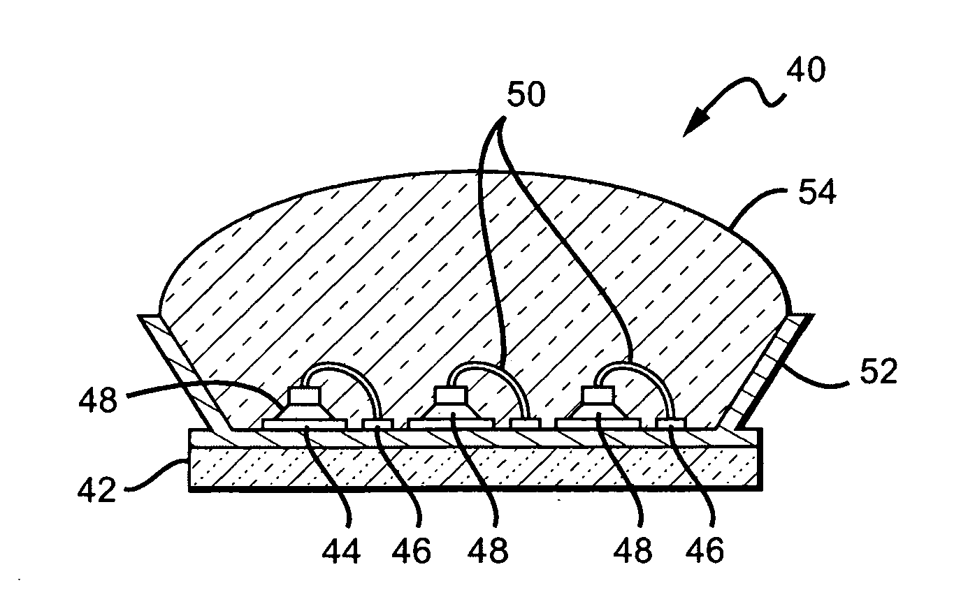
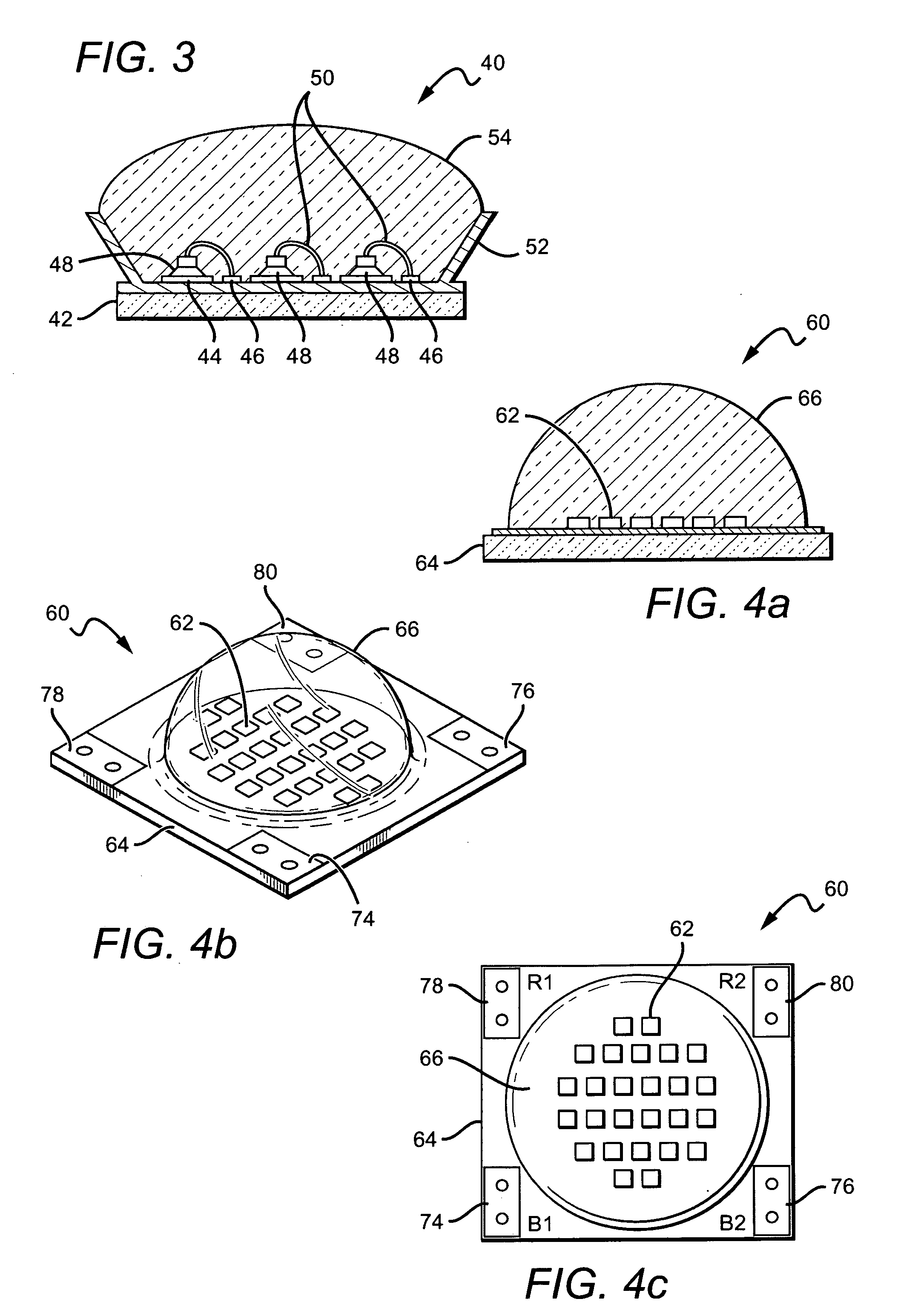
[0037]The present invention comprises a monolithic LED component having a plurality of LED chips mounted onto a submount to create a single compact optical source element. As used in the present application, monolithic refers to LED components wherein the LED chips are mounted on one substrate or submount. In some embodiments, at least some of LED chips are arranged in series electrical contact, with different embodiments providing multiple series connected LEDs, or combinations of series / parallel interconnect arrangements. The present invention allows for LED components to be designed and selected with a particular chip size and total LED emitting area to achieve the desired component size, and desired light output at an LED optimum current density per individual chip. This allows the LED components to be provided with the optimum efficiency at a particular cost. By flexibly choosing an LED chip size the present invention provides for a component that operates at the optimum voltag...


PUM


Abstract

An LED component according to the present invention comprising an array of LED chips mounted on a submount with the LED chips capable of emitting light in response to an electrical signal. The array can comprise LED chips emitting at two colors of light wherein the LED component emits light comprising the combination of the two colors of light. A single lens is included over the array of LED chips. The LED chip array can emit light of greater than 800 lumens with a drive current of less than 150 milli-Amps. The LED chip component can also operate at temperatures less than 3000 degrees K. In one embodiment, the LED array is in a substantially circular pattern on the submount.

Description

[0001]This application is a continuation-in-part of, and claims the benefit of, U.S. patent application Ser. No. 11 / 982,275 to Keller et al., filed on Oct. 31, 2007, and is a continuation-in-part of and claims the benefit of U.S. patent application Ser. No. 11 / 743,324 to Medendorp et al., filed on Sep. 27, 2007.[0002]This invention was made with Government support under Contract No. DE-DE-FC26-06NT42932 awarded by the National Energy Technology Laboratory. The Government has certain rights in this invention.BACKGROUND OF THE INVENTION[0003]1. Field of the Invention[0004]This invention relates to methods for solid state lighting and in particular compact monolithic solid state lamps comprising multiple lighting elements.[0005]2. Description of the Related Art[0006]Light emitting diodes (LED or LEDs) are solid state devices that convert electric energy to light, and generally comprise one or more active layers of semiconductor material sandwiched between oppositely doped layers. When ...

Claims


Application Information

Patent Timeline
Patent Type & Authority Applications(United States)
IPC IPC(8): H01L33/00H05B44/00
CPCF21K9/00H01L25/0753H01L2924/09701H05B33/0821H05B33/0857H01L2224/48247H01L2224/73265H01L2224/32245H01L2224/48091H01L2924/00014H01L2924/00H05B45/40H05B45/20H01L2924/00012H01L33/486H01L33/58
Inventor YUAN, THOMASKELLER, BERNDTARSA, ERICIBBETSON, JAMESMORGAN, FREDERICKDOWLING, KEVINLYS, IHOR
Owner CREELED INC
Why Eureka
Try Eureka